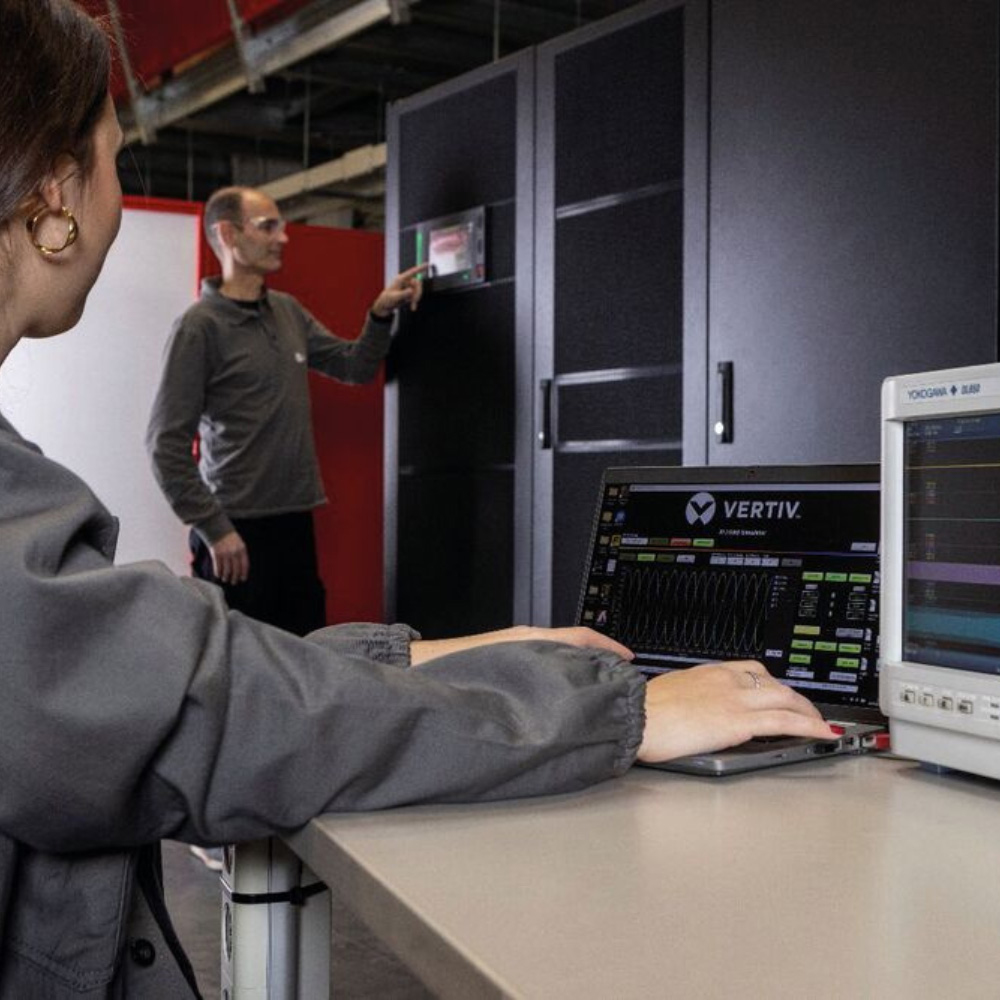
Prof. Dr.-Ing. Eckart Hoene, Chief Expert Power Electronics, Fraunhofer Institute for Reliability and Microintegration (IZM), Berlin, Germany
The potential numbers raise the profile of the material choices. As production volumes increase, material costs become a dominant factor in prices, as well as driving the environmental impact. Achieving the necessary volumes also means that manufacturing has to adapt: something as fundamental as the winding of a coil requires a different approach if production numbers are in the hundreds of millions.
Design for manufacturability
In a discipline as mature as power electronics, it is not unusual for a chain of different specialists to be involved during product development, from the concept, to the circuit diagram, components and control strategies, to the layout and defining of the bill of materials. The awareness of established and possible pro-duction methods needs to be considered ever earlier in this chain to enable the production of ever larger quantities.
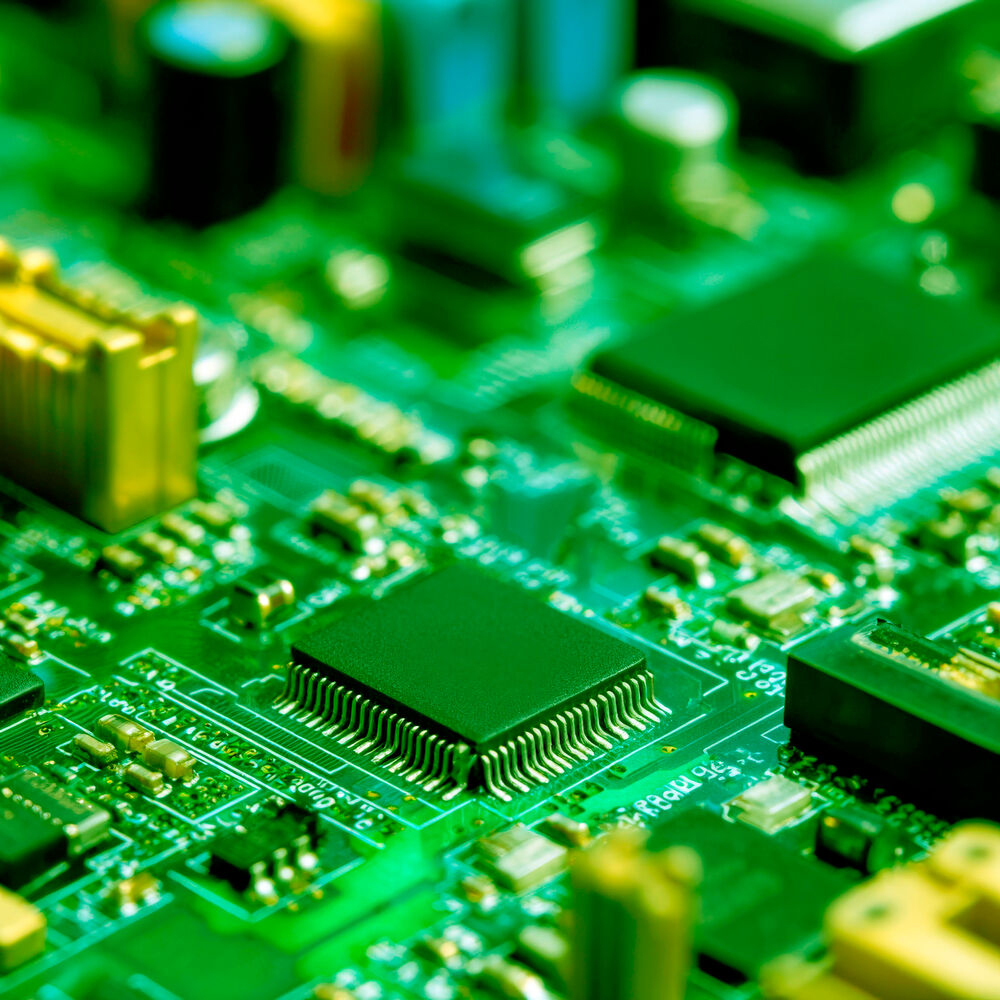
Of the mass production technologies for elec-tronics, few are as widespread as printed circuit boards (PCBs). Although PCBs have been around for decades, it is still possible to push the envelope. DC-DC converters for GPUs and TPUs, for example, can embed semiconduc-tors in the PCB, and include PCB inductors to make voltage regulation modules (VRMs) with reduced interfaces and conductor lengths, that are volume optimized and can handle high currents with low losses.
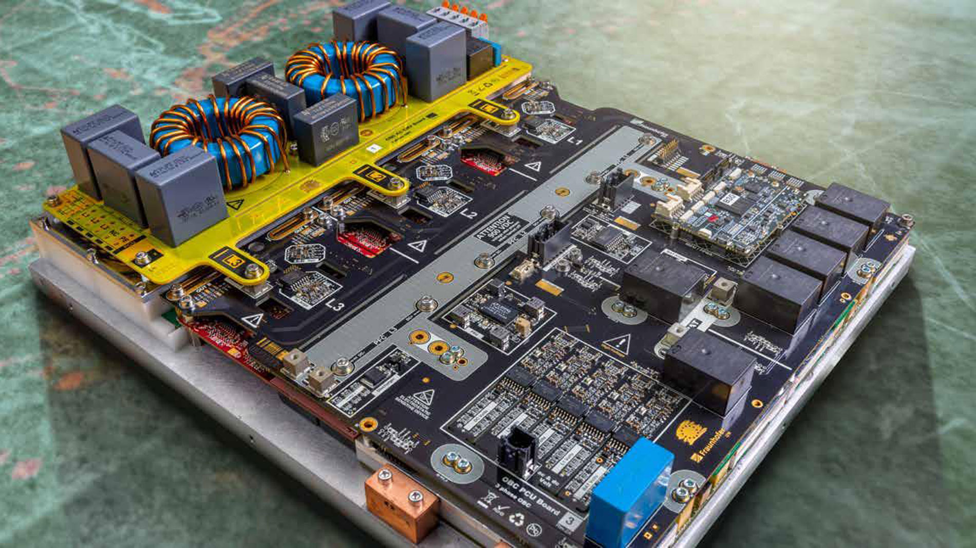
Inductors using PCB technology can also be applied at higher voltages. We have used these, for example, in a 22 kW onboard charger: if a designer knows they have that degree of freedom they can adapt the topology to shift from manual manufacturing – instead of winding a coil that needs through-hole technology and potentially even mechanical mounting – to something that is a surface mount device (SMD) that is easier for a machine to handle. PCB technologies are also already being used for traction inverters in the automotive industry, where there is both the commercial motivation and the engineering depth to make the most of such advances.
Economies of scale
Another way of improving the efficiency of manufacturing is to use larger PCB panels – up to 60 × 60 cm in large scale production – to produce many more units in parallel. (This is the same approach that the semiconductor industry has been using for years in increasing silicon wafer sizes.) By dividing the production steps by the number of units, the cost per unit decreases.
The same idea can be applied to manufacturing components, shifting transfer moulding from the common 10 × 30 cm size batch to 60 × 40 cm. This is a current research project – fi-nanced by a consortia of industry partners – at the Fraunhofer IZM. The close collaboration with industry is important. Input, guidance and accountability to industry partners helps meet real needs, not least ensuring the right production machines can be prepared, to smooth the transfer to practice.
The current challenge in the project is understanding the different shrinkage as the polymers of the larger batch sizes cure. Solving this ensures the transfer mould aligns correctly and reliably for the following stages of production. Otherwise, for example, the laser might not find the pad it expects on a chip.
Expanding the parameter set for further optimization
Enabling electrification contributes to the more efficient use of energy – one only has to compare the 25% efficiency of an internal combustion engine with the 80% efficiency of an electric vehicle. But more than this, power electronics is essentially about pushing the boundaries of that efficiency, to minimise the losses in the energy flow chain. Add in the push, particularly in automotive applications, to create solutions that are as small and light-weight as possible. This reduces the materials needed, which is good for the environment as well as the costs. Work has begun in looking more at the whole lifecycle: how a product is manufactured has an important role to play in how easily it can be reused or recycled. This becomes a further parameter to be optimized from the conceptual phase on. An important additional opportunity here would be to design to use more recycled materials, like copper or aluminium. Or – even when the raw materials are not economically or ecologically expensive – to look for oppor-tunities to use renewables, for example for the energy intensive growing of silicon carbide crystals.
The next horizon will be gathering more infor-mation about the carbon footprint or environmental price for different materials. This is a further parameter that could be considered for optimization, if the data were sufficient. There is an awareness already, and the signs are optimistic.