At this year’s ISSCC, the team of developers led by Professor Bernhard Wicht of Leibniz University Hanover presented a fully integrated power stage in GaN. The monolithically integrated half-bridge operates from 500 V and achieves switching frequencies of 6.25 MHz – a record performance. The group demonstrates the record circuit in a totem pole converter with power factor correction.
Galliumnitrid (GaN) is best known for its use in mobile phone chargers, but the requirements for power supplies for devices that consume more power, such as PCs, larger tablets or displays, are quite different. Prof. Dr.-Ing. Bernhard Wicht, from the Institute for Microelectronic Systems at the Leibniz University of Hanover, explains: “In contrast to the usual mobile phone chargers, which are specified for a power between 5 and 20 W, power supplies with 200 W have completely different requirements. It starts with the topology, because a power of around 200 W usually requires a DC link voltage. Specifically, this means that you first convert from the AC voltage to a 400-volt DC-link voltage and then step it down from there. In addition, power factor correction (PFC) is mandatory in such power supplies; the standards require it.”
He and his students have set themselves the goal of developing a power supply unit for the 200 W power class based on GaN. This would enable the power supplies used to date to be significantly smaller on the one hand, and to achieve a higher effciency on the other. Wicht: “And both are possible with GaN.” Wicht and his team of developers are thus addressing a market that is not without interest, because “grid-fed electronics consume TWh of energy annually,” Wicht continues.
The first step has been taken
At this year’s ISSCC in San Francisco, the developers presented a fully integrated GaN-on-SOI-based (silicon-on-insulator) circuit to be used in a power factor correction totem pole topology (TPPFC) that can handle up to 55 W. The fact that less than 55 W has been achieved so far is due to the selected TPPFC system and corresponding design.
GaN as a semiconductor material for ICs is not yet as mature as silicon and this also applies to the 650 V GaN-on-SOI technology from imec used for the development. “We still have to struggle with unpredictable process variations and unfavorable analog properties such as matching etc.,” Wicht continues. But: “In the meantime, we have developed concepts and solutions for this and are confident that the next test chip, which we are currently realizing, will achieve 200 W and even more functionality.”
Despite the initial difficulties, Wicht is convinced by the GaN-on-SOI technology, because this technology has advantages, for example, that both high-side and low-side can be implemented on a common substrate. Wicht continues: “GaN-on-SOI is really brilliant, because GaN is free of bipolar effects and with SOI various circuit functions can be integrated on-chip, leading to small parasitic elements, allowing for faster switching. I don’t think we would be able to break the record with 500 volts and 6.25 MHz without SOI.”
“With our half-bridge integrated in GaN and 500 V, we were able to achieve a frequency of up to 6.25 MHz. That is an absolute world record, no one has ever managed that before.”
High integration density, high clock frequency
The fully integrated 500 V power stage includes a level shifter, gate drivers and power FETs on a single die. In addition, very high clock frequencies can be used. The established players in the GaN market typically work in the 1 MHz range. “We actually went up to 6.25 MHz with our integrated halfbridge at 500 volts. Both values have been validated and that is still a world record,” says Wicht. In addition, the development is characterized by excellent waveforms, according to Wicht. “The high integration has greatly reduced the parasitic effects, and the inductive effects are also low, which in turn reduces ringing. This simply shows the potential of GaN.”
The GaN IC is used in a TPPFC system based on the TPPFC 1680 controller from Onsemi, so the overall system could not be clocked as high.
Further development is assured
Further development is being driven forward by the DFG (German Research Foundation) as part of the priority program “GaNius”. One of the issues here is to find out which clock frequency really makes sense from a technical point of view, “because it is now clear that we can clock very high”, Wicht continues. In addition, the focus is of course on integrating further functions, such as a closed control loop on the die. “Driving system integration using advanced packaging technologies is also an approach we are looking at. For example, we would also like to integrate the passive components,” explains Wicht. However, the first step is to get the most out of the monolithic approach.
Details from the ISSCC paper
The paper 31.10 with the title “A Fully integrated 500 V, 6.25 MHz GaN-IC for Totem-Pole PFC Off-Line Power Conversion« presents a TPPFC converter that benefits from a monolithic GaN-IC with a fully integrated half-bridge power stage in a 650 V GaN-on-SOI technology.
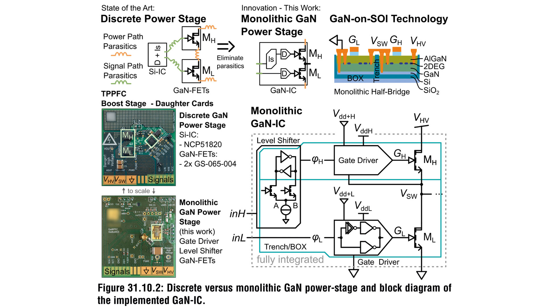
Figure 31.10.2: Discrete versus monolithic GaN power-stage and block diagram of the implemented GaN-IC. Image: ISSCC Digest/Leibniz University Hanover
A 650 V GaN-on-SOI technology utilizes trench isolation and buried oxides (BOX), allowing the integration of the entire power stage on one single die. Figure 31.10.2 (top right) depicts the cross-section. Besides the HV transistor, the technology offers a low voltage transistor, a 2DEG resistor, and a capacitor. A d-mode device is not available, and generally, no p-type device. The PCB photos in Fig. 31.10.2 show the monolithic ML/MH halfbridge daughter board and, for comparison, the discrete design used in the TPPFC system. The monolithic implementation reduces component count and footprint size. Figure 31.10.2 (bottom right) shows the GaN-IC of this work comprising split-path gate drivers and a half-bridge with equally sized 500 mΩ power FETs to ensure symmetric operation in positive and negative half-line cycles of the TPPFC operation. A cross coupled level shifter with robust HV capability interfaces the high- and low-side domains. The high-side rails VddH, Vdd+H are generated by bootstrapping from the low-side supplies VddL, Vdd+L.
With the lack of p-type devices, topology choice is crucial in GaN gate driver design. The implemented full-rail gate driver in Fig. 31.10.3 relies on a split-path approach with separately controlled paths for Mpu, Mpd. Each path consists of an RTL inverter followed by two subsequent push-pull stages showing tapered drive strength and mini mized static power consumption (RRTL = 59 kΩ). The push-pull stages employ n-type devices in the pull-up path, inherently limiting the output high-state to Vout,high ≤ Vin,high Vth. An enhanced supply voltage Vdd+ is applied to the respective stages, ensuring full turn-on of Mpu when the gate driver output GH/L is pulled high, resulting in full-rail driving. The gate driver achieves rise/fall times of 3.5/2.7 ns with less than 2 % overshoot, switching at 10 MHz, as shown in Fig. 31.10.3 (bottom left). The propagation delay is 8.8/6.4 ns for the rising/falling edge, faster than other comparable approaches. Monolithic integration significantly improves the power-FET gate loop. However, some inductance remains in the turn-on path; see Fig. 31.10.3 (top right). The gate driver facilitates a voltage tuning technique, allowing to adjust Vdd+ to limit the parasitic loop induced gate voltage overshoot at the power-FET gate. Based on the on-chip measurements in Fig. 31.10.3 (bottom right), Vdd+ = 11 V is selected as a trade-off between rising edge slope and overshoot.
Figure 31.10.2: Discrete versus monolithic GaN power-stage and block diagram of the implemented GaN-IC. Image: ISSCC Digest/Leibniz University Hanover
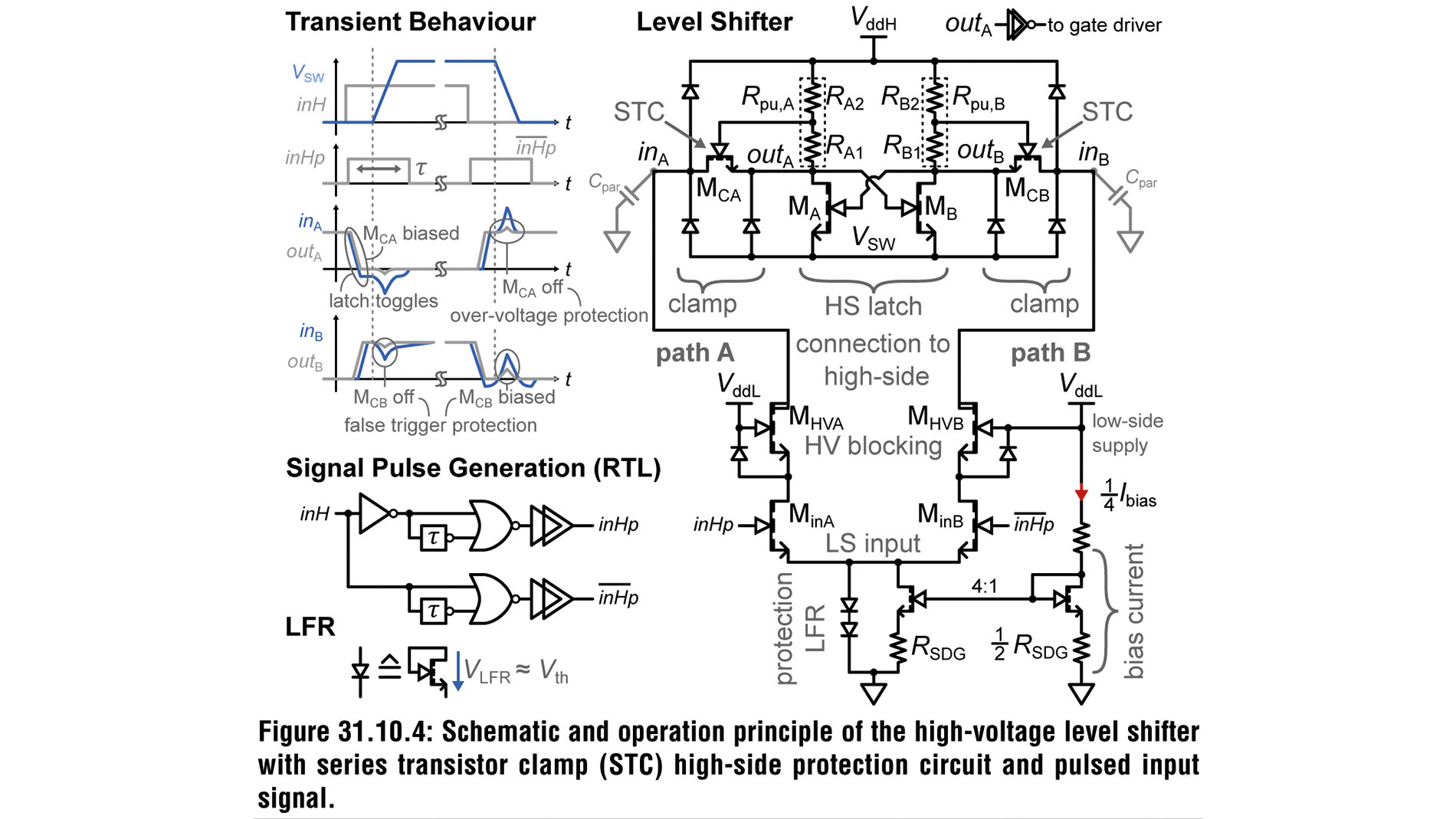
Figure 31.10.4: Schematic and operation principle of the high-voltage level shifter with series transistor clamp (STC) high-side protection circuit and pulsed input signal. Image: SSCC Digest/Leibniz University Hanover
Figure 31.10.4 shows the level shifter implemented on the GaN-IC. At the high side, a cross-coupled RTL-inverter latch holds the logic state. Directing a bias current Ibias (600 μA) through either MinA or MinB pulls inA or inB low, activating MCA/MCB. This pulls down the corresponding outA/B node, toggling the latch. outA is connected to the HS gate driver input via an inverter acting as a buffer. To minimize losses due to Ibias, the input signals are applied in a pulsed manner, accomplished by RTL logic and an R-C delay. Ibias is generated by a current mirror employing a source degeneration RSDG to account for threshold voltage variation. HV cascodes MHVA and MHVB, referred to VddL, and lateral field-effect rectifiers (LFR) protect the low-side circuits from the high voltage at inA/B. Due to the parasitic capacitance, Cpar at inA and inB (marked in Fig. 31.10.4), the HV transient at the switching node Vsw can cause critical over-voltage stress at the gates of MA and MB. As a key innovation of the proposed level shifter, a series transistor clamp (STC) formed by MCA and MCB protects MB and MA. Vdd is typically chosen close to the VGS,max rating of the GaN-FETs; hence, clamping to Vdd+VLFR is insufficient. The proposed STC achieves protection by reusing the pull-up resistors of the latch to control the gate of MCA and MCB, illustrated by the transient curves in Fig. 31.10.3 (left). For outA at high state (= VddH), MCA disconnects outA from inA with its source and gate nodes pulled to VddH via RA1, RA2 while MCB is activated to prevent false triggering by disturbance at inB. In lowstate (outA at Vsw), the STC limits V(outA) to (VddH – Vsw) · RA1/(RA1+RA2)–Vth, protecting the gate node of MB from over-voltages. The resistive divider ensures that the STC kicks in earlier, maintaining the max. ratings of MA and MB. Accounting for Cpar of up to 100 fF, RA1/RA2 and the widths ratio W(MCA)/W(MA) are chosen 2:1, similarly, for path B.
Figure 31.10.4: Schematic and operation principle of the high-voltage level shifter with series transistor clamp (STC) high-side protection circuit and pulsed input signal. Image: SSCC Digest/Leibniz University Hanover
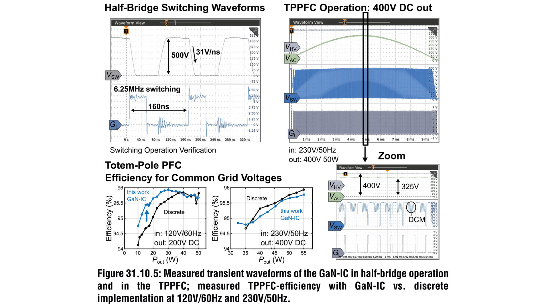
Figure 31.10.5: Measured transient waveforms of the GaN-IC in half-bridge operation and in the TPPFC; measured TPPFC-efficiency with GaN-IC vs. discrete implementation at 120V/60Hz and 230V/50Hz. Image: ISSCC Digest/Leibniz University Hanover
Figure 31.10.5 shows the transient measurement results of the switching GaN-IC. The half-bridge and, thus, the level shifter is verified to operate at 500 V and frequencies up to 6.25 MHz (upper left), achieving an average Vsw slope of 31 V/ns. The GaN-IC is applied in a TPPFC system based on the onsemi 1680 TPPFC controller, converting the AC input to VHV = 400 V (DC) (Fig. 31.10.5 right). The zoomed section shows the instantaneous AC voltage close to the peak of 325 V and the low-side gate voltage. Also, the DCM-related ringing of VSW is visible. The TPPFC is operated in two standard grid configurations and compared to the discrete power stage of Fig. 31.10.2 (center left): 120 V – 60 Hz (VHV = 200 V) and 230 V – 50 Hz (VHV = 400 V). The efficiency curves in Fig. 31.10.5 (bottom) confirm the higher effciency of the GaN-IC at lighter loads as it is switching-loss optimized.
The GaN-IC is fabricated in a 650 V GaN-on-SOI technology using an active area of 6.6 mm² (Fig. 31.10.7). The IC utilizes the advantages of monolithic GaN integration, providing miniaturization, lower internal and external parasitics and high design flexibility.
Figure 31.10.5: Measured transient waveforms of the GaN-IC in half-bridge operation and in the TPPFC; measured TPPFC-efficiency with GaN-IC vs. discrete implementation at 120V/60Hz and 230V/50Hz. Image: ISSCC Digest/Leibniz University Hanover
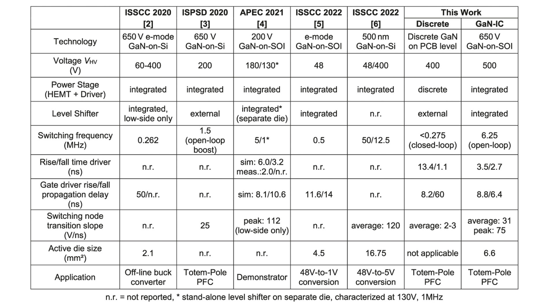
Figure 31.10.6: Comparison of the implemented GaN-IC and its sub blocks with the discrete PCB power stage and state-of-the-art design. Image: ISSCC Digest/Leibniz University Hanover
Figure 31.10.6: Comparison of the implemented GaN-IC and its sub blocks with the discrete PCB power stage and state-of-the-art design. Image: ISSCC Digest/Leibniz University Hanover
Europe and semiconductors
“The costs for having a test chip manufactured are around 30,000 euros for us, and even more than 100 k euros, for advanced nodes,” explains Prof. Dr.-Ing. Bernhard Wicht, who works at the Institute for Microelectronic Systems at the Leibniz University of Hanover. And that is precisely where a major problem lies, because universities cannot afford this often. That is why Wicht is convinced that this point must also be addressed by the EU or Germany, i. e. financial support from the government. “When I talk to colleagues from universities in China or Taiwan, they either don’t have to pay anything or a minimal price, the rest is subsidized by the state. While we are still discussing the costs here, whether we can make a chip, they have already made 10 chips.” This is also important because the European Chips Act is also about the universities training the corresponding semiconductor developers. Wicht explains that his university, thanks to its reputation, “attracts great people but currently held back from reaching its full potential. Because the costs of chip production are a big problem for European/German universities.”