HOOP – the Path to Efficient Power Supply for High Performance Computing
6 May 2025
According to Visualcapitalist, it took just over a month for ChatGPT to surpass 50 million users. The run is unique, as are the demands on computing power and the energy required to achieve it.
And the growth of AI and the increasing demand for computing power continues unabated – which is a problem in that a single high-performance GPU already requires up to 1000 W of power. In one of its recent forecasts, Goldman Sachs Research predicts that global energy demand for data centres will increase by 50 percent by 2027. James Schneider, Senior Equity Research Analyst at Goldman Sachs Research, explains: “Compared to 2023, energy demand will increase by as much as 165 percent by the end of the decade.” Goldman Sachs Research estimates that the global data centre market currently requires around 55 GW of power. This power consumption is made up of workloads in the cloud (54 percent), plus traditional workloads for typical business functions such as email etc. (32 percent), plus AI (14 percent).
Looking ahead, the analysts predict that electricity demand will rise to 84 GW by 2027, with AI accounting for 27 percent of total demand, cloud 50 percent and traditional workloads 23 percent. Although Goldman Sachs Research adds that the figures may be overestimated by 9 to 13 GW because AI is not developing quite as fast as expected, either way, the power requirement is gigantic.
But how?
To meet the huge power demand, dozens or hundreds of PoL (point of load) converters are often operated in parallel to increase the output current. In order for the multi-phase converters to work efficiently, it is essential that the current is evenly distributed across all phases. If this is not the case, unbalance will cause overloading of individual phases and reduce component life.
There are several approaches to ensuring this balance. These include decentralised voltage control, where each phase has its own controller that monitors and adjusts the output voltage. Interleaved topologies are also used, where the switching times of each phase are staggered to reduce current ripple and increase overall power. There is also the option of monitoring the system centrally with a current sharing controller. In this case, a central controller monitors the currents of each phase and adjusts the control signals accordingly to ensure an even load distribution.
Regarding the last option, a central controller, Prof. Dr.-Ing Bernhard Wicht from the Institute for Microelectronic Systems at the Leibniz University in Hanover explains that, »as the number of phases increases, the complexity of current sharing control increases significantly. Therefore, an inherent property for automatic current balancing in DC-DC converters would be very helpful«.
And it is precisely this approach, i.e. automatic compensation, that Professor Wicht, together with Professor Yan Lu from Tsinghua University, Beijing/China and his research team from China (Zhiguo Tong, Junwei Huang, Zhewen Yu and Rui P. Martins from the University of Macau/China and Tsinghua University, Beijing/China, and Xiangyu Mao from UM Hetao IC Research Institute, Shenzhen/China) presented at this year’s ISSCC.
HOOP-converter
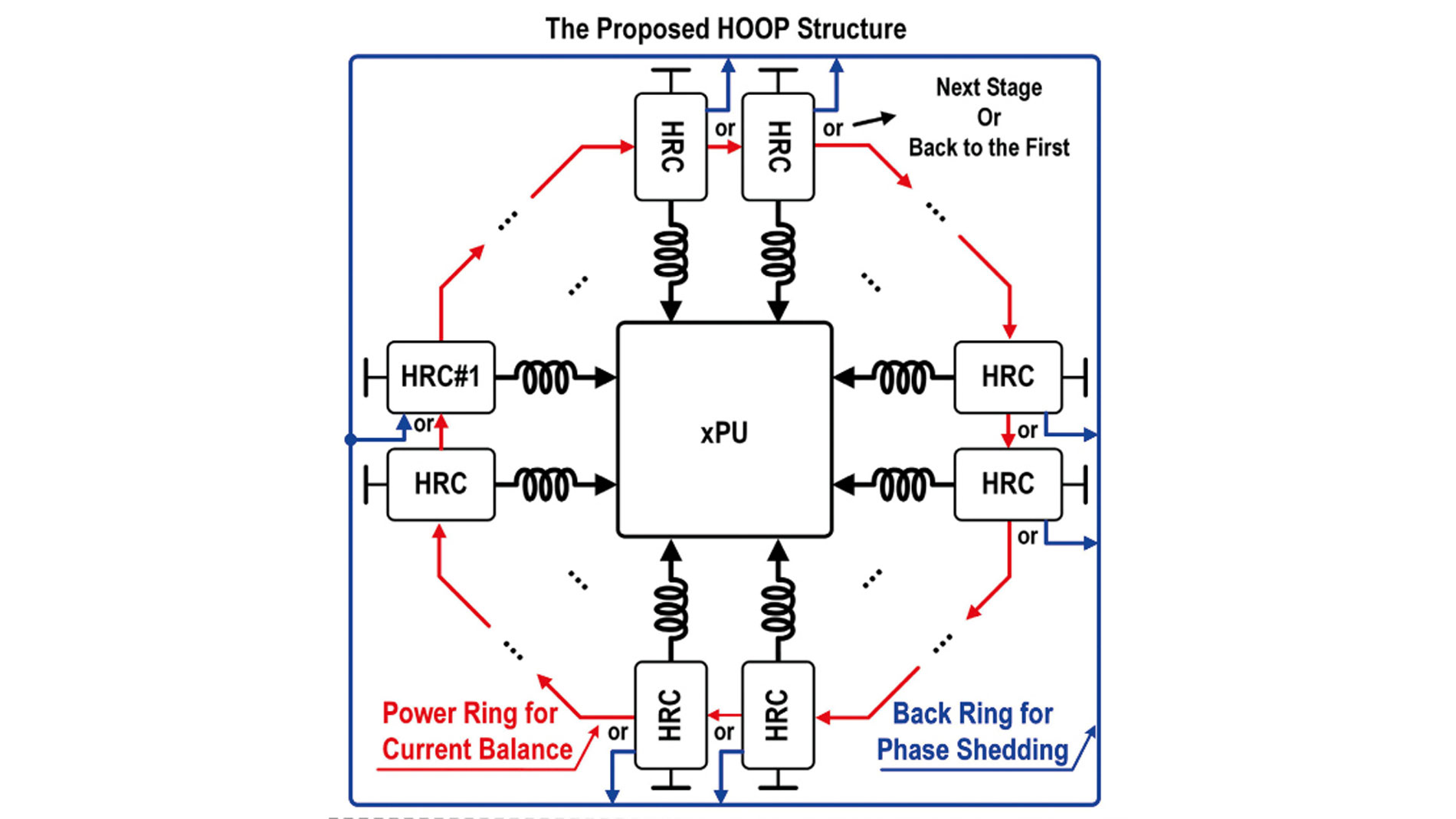
The HOOP structure. Images: IEEE
The so-called HOOP converter (Hybrid Converter with a Power Ring (O) for Current Balancing and a Back Ring (O) for Phase Shedding for Computing Power Delivery) is a hybrid converter with a power ring for current balancing and a back ring for phase shedding. Its ring-shaped arrangement of Hybrid Ring Cells (HRC) around the loads enables automatic current balancing and makes it easy to expand to any number of converter phases.
In this approach, a small, fixed proportion of the inductor current is taken from each branch and passed on to the next branch. As a result, each branch takes some current from the previous branch and gives some to the next. So if there is a current mismatch between two neighbouring inductors, this mechanism of continuous current transfer from one phase to the next automatically balances the differential currents. The additional ‘back ring’ allows phases to be selectively switched off to optimise system efficiency under varying load requirements. At low loads, it is inefficient to keep all phases active as this results in unnecessary switching losses and lower overall efficiency. By shutting down certain phases, the inverter reduces switching losses and dynamically adapts to the current power demand. The back-ring coordinates this process by putting the inactive phases into sleep mode and reactivating them when the power demand increases. This mechanism helps to minimise energy consumption and maximise converter efficiency over a wide range of load conditions.
Current drawn from each cell can be routed either to the next cell or back to the first cell to ensure efficient operation under varying load conditions. This self-balancing ring structure greatly simplifies the power supply layout and, by supplying power to the xPUs vertically, significantly reduces I²R losses on the PCB and in the enclosure.
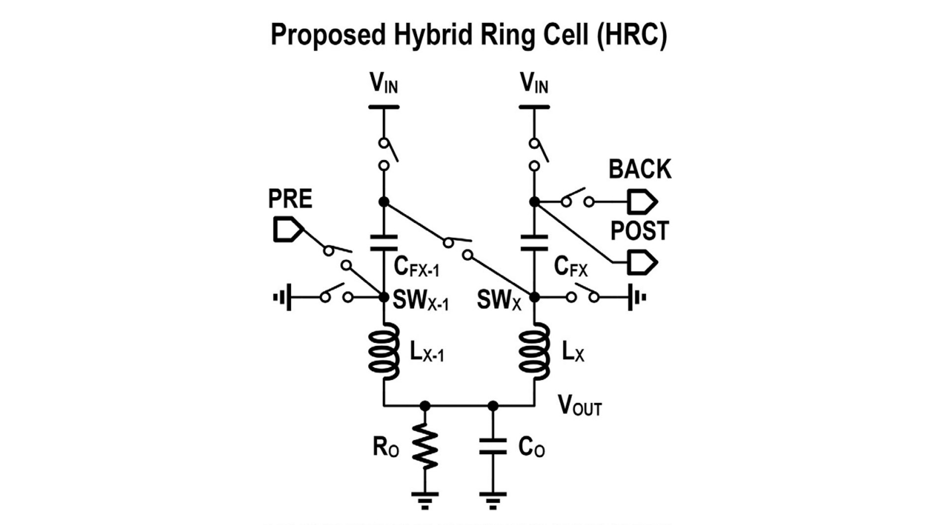
To illustrate the concept, a module has been developed using the proposed HRCs, where each HRC contains all the power transistors, drivers, bootstrap circuitry, and controllers on a single chip, plus two flying capacitors and two inductors. The HRC operates in three phases:
Phase βX: Inductor LX discharges the preceding capacitor CFX-1.
Phase γX: LX is demagnetised.
Since the capacitor CFX-1 is used in the phases αX-1 and βX, the two phases must be offset in time. The duty cycles of αX and βX are identical and correspond to the duty cycle DT. By applying the volt-second balance principle (which states that the average voltage across an inductor in a switching cycle must be zero to ensure stable operation) to the inductors and the charge balance principle to the flying capacitors, it can be deduced that the inductor currents automatically equalize and the flying capacitor voltages also stabilize. Despite the lack of a dedicated charging path to maintain a fixed voltage on the flying capacitors, a natural balancing loop causes the flying capacitor voltage to stabilize at VIN/2.
“The HOOP module presented enables automatic and uniform current matching across the phases and is scalable as required.”
Comparison with other approaches.
In a HOOP module example, three HRCs have been connected in parallel. The POST pin of each chip is connected to the PRE pin of the next chip, while all BACK pins are connected to the PRE pin of the first chip. There are two modes of phase cutting:
Active mode: In this mode, each HRC can either connect to the next HRC or to the first HRC to form a complete current equalization loop.
Sleep mode: The HRC is inactive, increasing efficiency at lower output currents.
There is also a transient mode in which all power branches operate in α-phase to increase the currents in all the inductors simultaneously, thus improving the response to load steps.
“To provide high currents, many point-of-load converters operate in parallel - but the more phases there are, the more complex the power distribution becomes. Precise current balancing requires targeted control, which becomes a real challenge as the number of phases increases.”
Thanks to the automatic current compensation function, the HOOP can be controlled with a simple PID control in voltage mode without having to measure the inductor currents. The duty cycle is generated by the first HRC chip and passed on to all HRCs. As neighbouring converters operate out of phase, the propagation delay is not critical. Depending on the load current and load changes, the HRC chips switch between four modes according to defined rules.
Structure of an HRC.
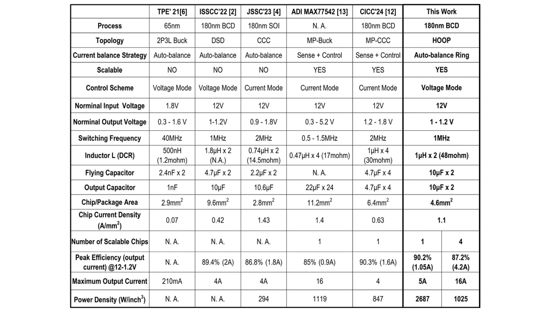
The HRC’s start-up waveforms show automatic current equalization and voltage stabilization of the flying capacitors over the entire VIN range. At an output current of 3 A, a single HRC chip has a current deviation of only 40 mA and an output voltage ripple of 18 mV. Despite significant differences in inductance values (L1 at 2 µH and 204 mΩ, L2 at 1 µH and 48 mΩ), the inductor currents show a deviation of only 90 mA, demonstrating the tolerance of current matching to path impedances. When the load changes from 300 mA to 3 A within 80 ns, the HRCs respond in transient mode, with all inductor currents increasing together. The inductor currents of the HRCs in sleep mode also help to charge the output capacitor, accelerating the recovery of the output voltage and reducing the voltage drop by 50 percent. The HOOP module achieves peak efficiency of 90.2 percent at 1A for a single chip and 87.2 percent at 4.2A for four chips, with a maximum output current of 16A. With four HRCs operating at 12V to 1V and the output current set to IOUT, the current transmitted through the ring path is only IOUT/8, with a duty cycle of 1/12. At 4A output current, this loss is only 0.06 percent of the output power. Compared to current designs, this HOOP module provides an easily scalable, automatically current-equalized solution with high power and current density.
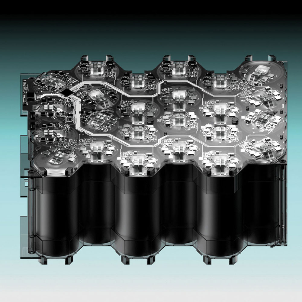
The chip is manufactured using a 0.18 µm BCD process and occupies an area of 4.56 mm² on which two 10µF (0402) capacitors are mounted. A four-chip HOOP module occupies an area of 16 × 16 mm, with all components on the top of the board and the load at the bottom, demonstrating its suitability for vertical power applications.