Prof. Dr.-Ing. Thomas Basler, Power Electronics, Faculty of Electrical Engineering and Information Technology, Chemnitz University of Technology
The first step in meeting all our energy needs from renewable sources is in the saving of electrical energy. Power semiconductors are already contributing here, from LED lighting, to variable speed drives for pumps, motors, and industry. Advances in power electronics have achieved efficiencies which mean that, despite strong increases in electrified applica-tions, overall electricity consumption did not increase. Some studies state a further potential saving of 22% of atmospheric emissions through the application of power electronics.
Improving price-performance points
Meeting the high demand on both sides of the supply and demand equation starts with improving the performance of the chips. Lower conduction and switching losses, – such as with the improved RDS(ON) of the second generation of trench gate SiC MOSFETs – helps increase the number of chips per wafer. This enables delivering more devices from the fabrication plants, and ultimately reduces price-performance points.
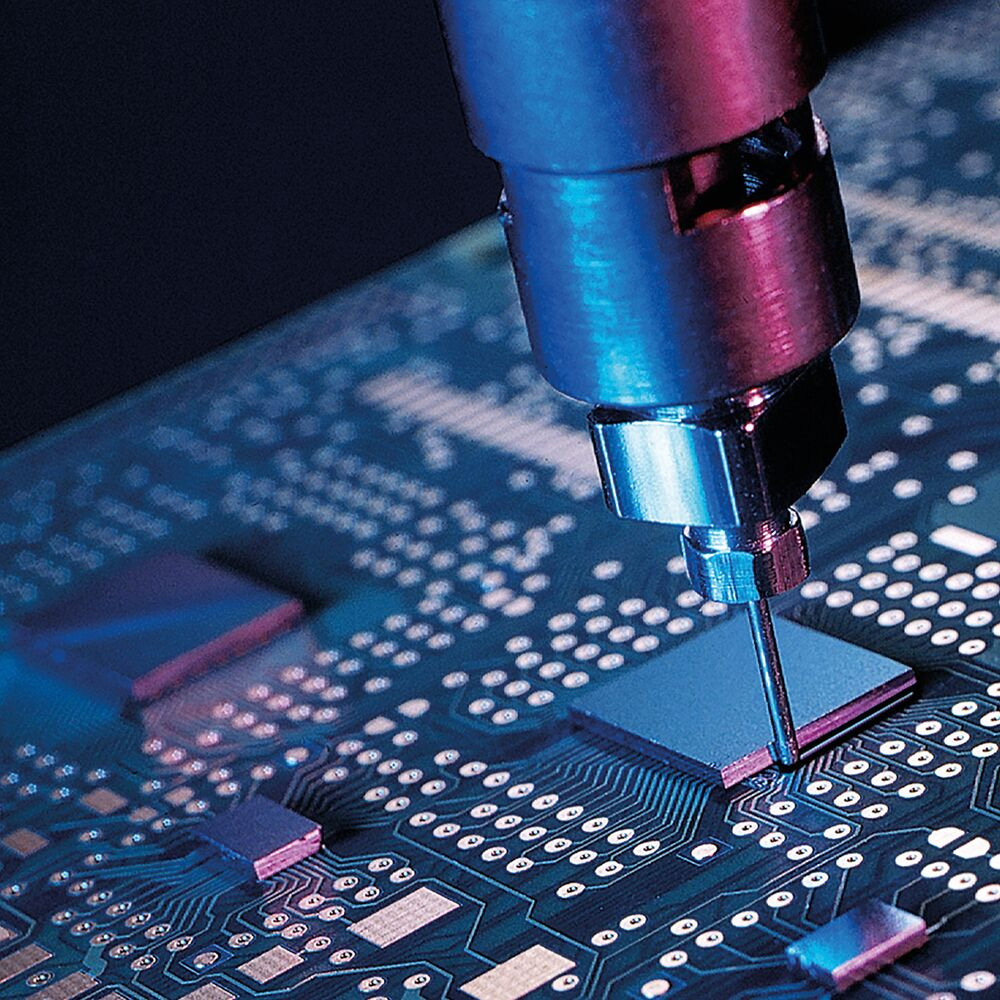
There are exciting developments in packaging, where new housings and materials are coming into play. And also new front-side interconnection technologies, such as for the front-side-only connection required for lateral GaN devices or clips. Foils and copper bond wires also offer interesting perspectives for getting the current out of even smaller chips. One trend is an increase in the variety of moulded discrete devices, such as small and larger half-bridge housings, or the many new solu-tions using top-side cooling. These use less material, are cheaper than the corresponding frame modules, and can be used in modular, self-designed parallel configurations (as is the case in Tesla EVs).
Other drivers come from increasing the range of applications for wide bandgap devices. For example, its low switching losses influenced the choice of SiC for achieving new levels of efficiency for solar inverters. But now we are seeing interesting possibilities for wind turbine applications, and traction applications where SiC MOSFETs in the 3.3 kV power module class could be used, significantly increasing efficiencies over today’s IGBT solutions. The ever improving reliability is also important: In the case of traction applications these systems are in use all day over a 30- to 40-year lifespan. This, for example, has been achieved using sintering on the back of the chips, and copper-based interconnection technologies on the front.
Challenges for testing
One of the biggest challenges is proving the reliability of the combinations of new chip, new packaging, and new interconnection technologies. Power cycling tests are most important, but this means improving the testing methodologies, or using innovative testing procedures, such as including new tempera-ture-sensitive electrical parameters as part of the power cycling test of GaN HEMTs. New tests are also needed, particularly dielectric testing in the form of a gate switching stress test for SiC devices, to gauge the gate oxide stability. This was not a mode that needed to be qualified for silicon devices, but in the meantime, it is mentioned in the ECPE’s AQG-324 testing standard for automotive power modules.
Often this is driven by the needs of the demanding applications, and not least by time pressure to get a solution to market. This has led to the theoretical understanding of SiC and GaN lagging behind Si-based counterparts, and the need to standardise tests for SiC and GaN to get reliable, comparable results.
Trade-off between effort and performance
Of course, new is not always better in all respects. The much smaller chip sizes and active thicknesses of SiC devices, for example, mean they reach very high temperatures and their failure limits much faster than IGBTs under short circuit conditions. And, despite all the hype around SiC and GaN, it is often silicon IGBTs that are available to meet the immediate demand for energy transition and electrifica-tion. Obviously, this will change as the capacity of SiC and GaN fabs increase in the coming years. IGBTs are also likely to remain dominant in high voltage and high current applications, like DC energy transmission. Or for applica-tions where cost, rather than space and losses, are the main driver, such as in variable speed drives in industry, or where costs are a big issue, such as in mass market EVs with moderate drive power.
There are also possibilities in hybrid tech-nologies, combining silicon carbide to ensure low losses for light load conditions with the beneficial I-V curve of Si bipolar devices at higher currents. This is under discussion for EV applications. Further, there are already multi-level power modules on the market combining the advantages of IGBTs at positions with lower switching frequency and SiC MOSFETs for positions needing higher switching frequency.
Improving capacity and yield
As noted, investment in new fabrication plants and increasing the yields per wafer are important in boosting the supply, to meet mushrooming global demand. In this respect, there are investments and advances in manufacturing silicon carbide, but, in the case of SiC, important work is also being done in splitting technologies to use the raw wafer for more than one pro-cessing run. A 1200 V class SiC chip only needs to be 10 µm thick, but ease of han-dling in the fab needs it to be 10- or 20-times as thick, and a raw 6” wafer is typically 350 µm. Nowadays, up to 60% of the wafer – which is the largest part of the cost of a SiC chip – ends up removed by backgrinding. A successful splitting technology would mean being able to use the raw material two or more times, and reducing device prices significantly.
The PCIM Europe 2024 – celebrating our success
There are a lot of new device and package concepts to learn about at this year’s PCIM Europe conference, as well as solutions to explore at the exhibition. And there are many more current issues and problems to discuss.
The growing numbers attending PCIM Europe events shows the increasing engagement in our community. In wider society, while there is awareness of wind turbines and photovoltaic power, there is little awareness of the vital supporting role that power electronics plays in enabling everything: from LED lights to electric mobility, and from renewable generation to the grid. Even the AI hype would be unthink-able without power electronics for supplying the power to the servers. The general public doesn’t (yet) know the importance and responsibility power electronics has in realising the potential of renewable energy and electrification in the fight against the upcoming climate disaster.