For 6G, frequencies between 7 GHz and the terahertz range will be used for the various bands to achieve the desired data rate of around 1 Gbps. These frequencies are not even feasible for GaN, as GaN devices can operate efficiently at frequencies in the MHz range. And in power electronics, higher frequencies could further extend the advantages that GaN and SiC have already made possible, i. e. even smaller passive components, even higher power density, faster response times, and even higher efficiency.
Accordingly, there are several promising developments aimed at further increasing switching frequencies. A variety of approaches are being pursued, including the use of new semiconductor materials such as GaN-on-SOI/GaN-on-TRSOI or UWBG (ultra-wide bandgap) materials such as AlGaN or diamond-based semiconductors. But not only new materials are being experimented with, new packaging technologies and new topologies (e. g. MMC modular multilevel converters) are also being explored.
E-mode GaN MOSHEMT transistors on a 300 mm GaN-on-TRSOI engineered substrate
At the last IEDM, Intel announced breakthroughs in GaN-on-TRSOI technology. The company unveiled the industry’s first high-performance scaled E-mode GaN MOSHEMT (metal-oxide-semiconductor high electron mobility transistor) transistors fabricated on a modified 300 mm GaN-on-TRSOI substrate.
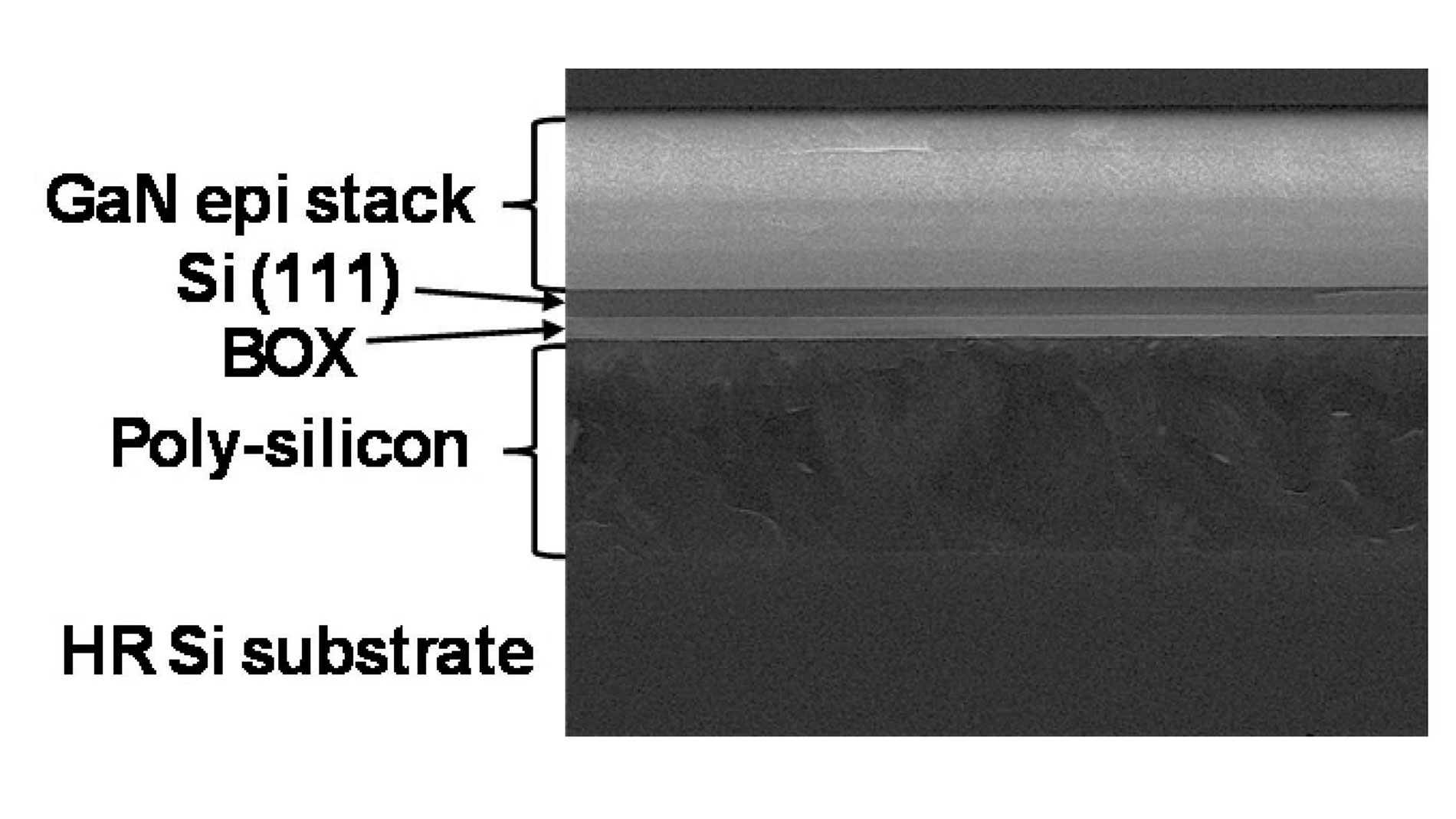
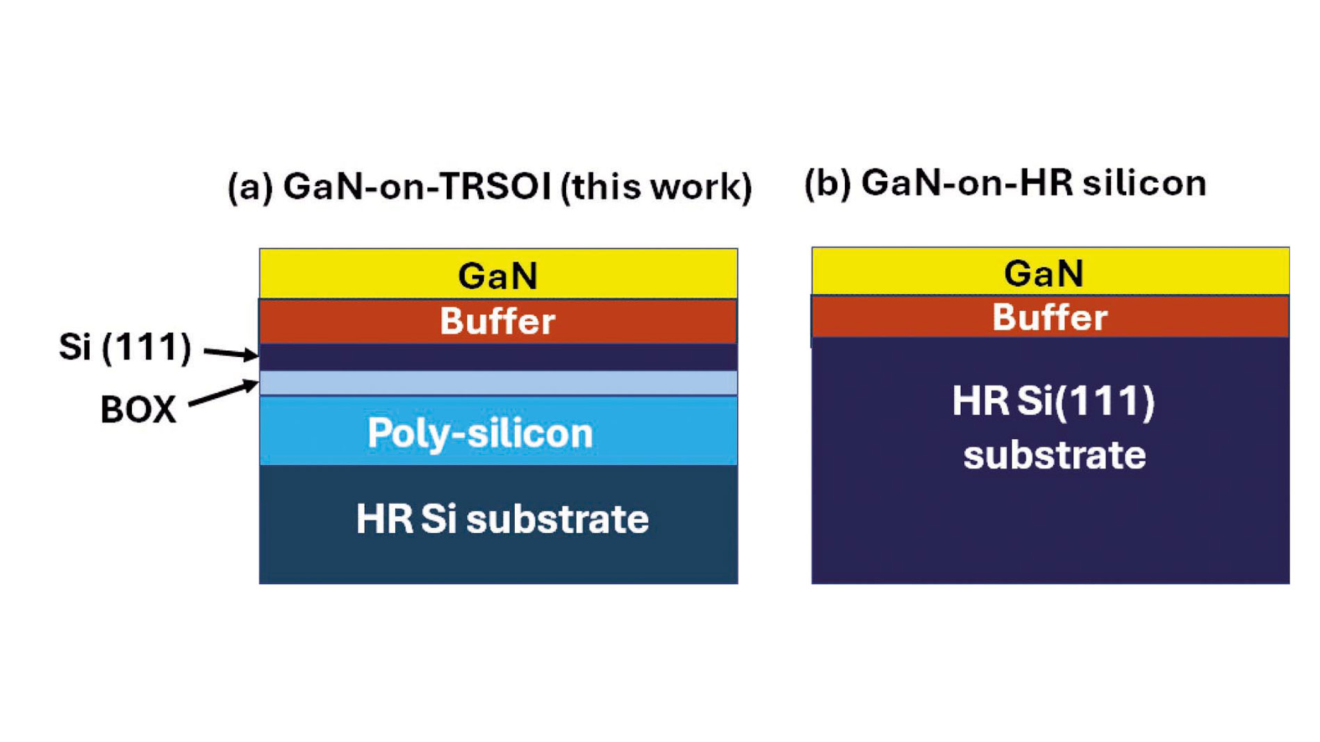
The new process is an evolution of Intel’s GaN-on-Si(111) technology, which has been used to fabricate scaled high-k dielectric E-mode GaN MOSFETs. In the previous process, the GaN epi stack was grown directly on the high-resistance (HR) silicon substrate. In the new process, the GaN epi stack grows on the modified 300 mm TRSOI substrate. This substrate consists of several layers: the first is a thin Si(111) layer, which enables the epitaxial growth of GaN. This is followed by a buried oxide (BOX) layer, which provides electrical isolation and reduces parasitic capacitance. This is followed by a trap-rich polysilicon layer (a polysilicon layer with many defects) to eliminate stray charges at the interfaces with the BOX layer and the HR silicon substrate. The TRSOI substrate is completed by the aforementioned HR-Si substrate. With the new TRSOI substrate, significant progress can be achieved. According to Han Wui Then, Senior Principal Engineer at Intel, the effective resistivity of the GaN epitaxial stack on a 300 mm GaN-on-TRSOI substrate is about four times higher than on a typical GaN-on-HR-Si substrate. The trap-rich polysilicon layer, in turn, enables 10 dB suppression of second-harmonic distortion, which improves signal linearity. He concludes: »These results represent an important advance for the use of 300 mm GaN in applications such as RF switches and millimeter-wave radio-frequency applications, for example, in the E, W and D bands.«
The paper for the IEDM states: »The 300 mm gate-last integrated process flow at Intel employs MOCVD GaN epitaxy, high-k gate dielectric, regrown epi source/drain, and Cu backend interconnect to enable GaN transistor scaling to 30 nm channel length. The process makes possible GaN MOSHEMT transistors of various different device architectures to be fabricated and integrated on the same wafer.«
Various different devices architectures
The 300 mm gate-last integrated process flow at Intel employs MOCVD GaN epitaxy, high-k gate dielectric, regrown epi source/drain, and Cu backend interconnect to enable GaN transistor scaling to 30 nm channel length. The process makes possible GaN MOSHEMT transistors of various different device architectures to be fabricated and integrated on the same wafer. The following part describes the results achieved for each of these GaN MOSHEMT devices.
30 nm Single-Gate GaN MOSHEMT on 300 mm GaN-on-TRSOI: A single-gate enhancement-mode high-k gate dielectric GaN MOSHEMT transistor has been fabricated on the 300 mm GaN-on-TRSOI wafer. Electrical characteristics reveal enhancement mode operation, drain current (ID) drive currents as high as 1 mA/µm, and an ON/OFF ratio of approximately 1010. The RF switch figure-of-merit (RON×COFF) for a 30 nm gate length device is an impressive 80 femtoseconds (fs). The transistor also exhibits a drain breakdown voltage (BVDS) of up to 66 V, with a breakdown field of 1.3 MV/cm.
30 nm Source-Field Plated GaN MOSHEMT on 300 mm GaN-on-TRSOI: A source-field plated enhancement-mode high-k gate dielectric GaN MOSHEMT transistor has been developed, featuring a submicron (100 nm) field-plate that adds minimal parasitic capacitance. This design effectively controls the drain field, as evidenced by the I-V characteristics, which show high current drive exceeding 1 mA/µm and the ability to handle drain voltage swings up to 12 V. Small-signal RF performance demonstrates high cut-off frequencies, with fT reaching 190 GHz and fMAX exceeding 500 GHz.
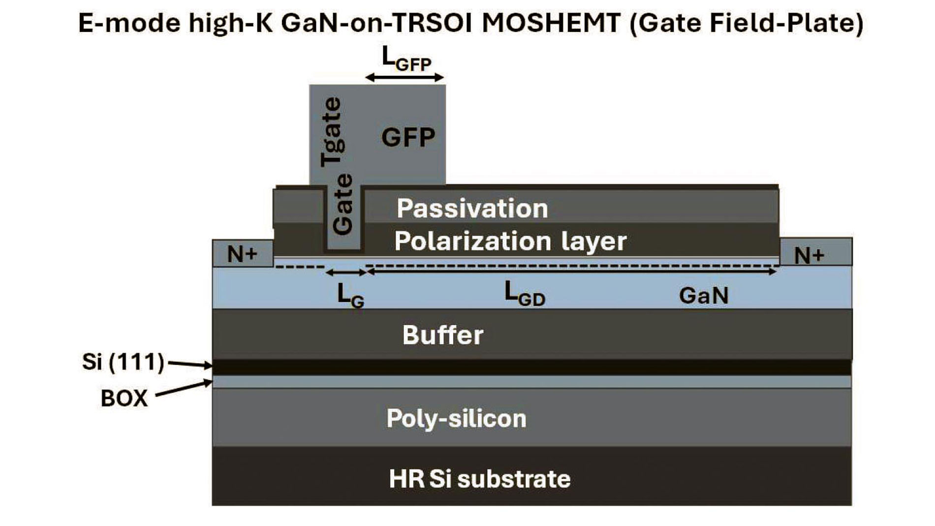
30 nm Gate-Field Plated GaN MOSHEMT on 300 mm GaN-on-TRSOI: The gate-field plated enhancement-mode high-k gate dielectric GaN MOSHEMT transistor exhibits pulsed I-V responses comparable to the source-field plated variant. The data indicates no degradation under quiescent conditions of Q (0 V,6 V) and a manageable 12 percent degradation in knee current under other specified conditions.
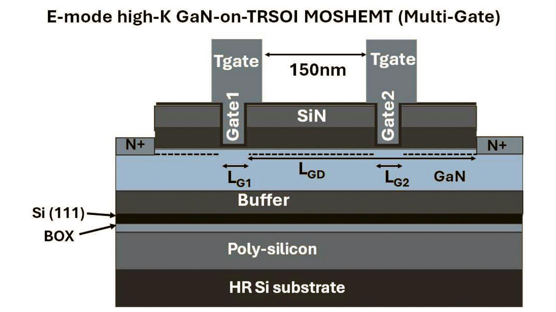
30 nm Multi-Gate GaN MOSHEMT on 300 mm GaN-on-TRSOI: A multi-gate (two-gate) enhancement-mode high-k gate dielectric GaN MOSHEMT transistor has been fabricated, with each gate having a 30 nm length and a gate-to-gate separation of 150 nm. This compact configuration, achievable in a 300 mm fabrication environment, is advantageous for implementing compact stacked RF switches, cascodes, and bi-directional switches. The ID-VD characteristics demonstrate improved short-channel effects and knee voltage, with high current drive up to 1.2 mA/µm. Transfer characteristics show modulation by the first gate potential and gating action by the second gate potential, achieving low RON of 590 ohm-µm in the fully-ON state and minimal leakage in the OFF state.
Intel is convinced that these advancements in 300 mm GaN-on-TRSOI technology represent significant progress in semiconductor technology, offering enhanced performance and integration capabilities for next-generation power delivery and RF electronics applications. The IEDM paper states: »Our work demonstrates for the first time high-performance scaled GaN MOSHEMT transistors fabricated on a 300 mm GaN-on-TRSOI engineered substrate. We have shown that the superior performance of scaled GaN MOSHEMT devices can be replicated on such novel engineered substrates. We have also demonstrated that various device architectures with and without gate/source-field plates and multiple stacked gates can be implemented and integrated on a 300 mm GaN-on-TRSOI wafer. Advanced engineered substrates can potentially achieve better performance in RF and power electronics by reducing signal loss and achieving better signal linearity and enabling advanced integration schemes that may be realized through backside substrate processing.« st