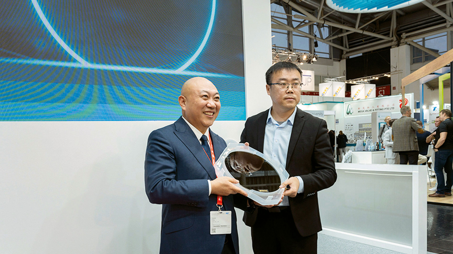
Anyone who wanted to see what the future of SiC production might look like in a few years’ time had the opportunity to do so last November at electronica 2024 in Munich. SICC presented the world’s first n-type SiC wafer with a diameter of 300 mm. Even if the exhibited piece was reportedly 1 mm thick for transport reasons, in industrial reality the thickness of such a wafer is likely to be closer to 500 nm. SICC plans to start producing 300 mm SiC wafers in small volumes as early as 2027.
»We want to continuously reduce the material costs per unit area by increasing the substrate size,« explained SICC Chairman Yanmin Zong at the presentation in Munich. He assumes that some of the leading SiC component manufacturers could be prepared to invest in 300-mm-lines in the next few years in order to reduce their production costs, but he also thought it possible that start-ups could see an advantage in starting with larger wafer diameters.
Perhaps the SICC Chairman’s ideas would sound more realistic if the overheated SiC market of recent years still existed. At a time when the total volume of the SiC component market was estimated at 10 billion dollars in 2029 and there was talk of annual growth rates of 25 percent between 2023 and 2029. Perhaps one or two SiC MOSFET manufacturers would then really have considered whether a switch to 300 mm would not make sense.
But those days are in the past. According to Poshun Chiu, Senior Market & Technology Analyst at Yole Group, the growth of the SiC market has slowed down so much, particularly due to the weak e-car market, that previously announced conversions from 150- to 200-mm-lines have now been postponed and these lines are not expected to enter the market until the end of this year or 2026.
According to Chiu, only two manufacturers are currently producing on 200 mm SiC components: Wolfspeed and Infineon Technologies. Wolfspeed announced this step in May 2019 at PCIM Europe. The corresponding construction work began in September 2019 and production started at the end of 2021, beginning of 2022. Ex-CEO Gregg Lowe began discussing the current production figures in the 200-mm-range in the quarterly reports since the beginning of 2024.
Talking to Wolfspeed employees, the migration from 150 to 200 mm proved to be quite challenging. Essentially, the problems can be reduced to one topic: Size matters! Everything had to be managed in larger machines and premises. The critical point here was ion implantation. The »particle accelerators« required for this are much larger than for 150 mm. The holding tools, which accompany the 200-mm-wafers through the production process, apparently also showed a higher shrinkage than originally expected. And then there was epitaxy, the most important process for passivating the defects in the wafers.
Wolfspeed got the problems under control with its suppliers and the corresponding manpower and, according to Yole’s estimates, will produce SiC MOSFETs worth around 60 million dollars on its 200-mm-lines in the first half of 2025. Infineon, for its part, only started supplying SiC products from its 200-mm-line in Villach in the first quarter of this year. According to Chiu, the contribution of the 200-mm-lines to Infineon’s SiC sales, which totalled around 190 million dollars in the first quarter, is likely to be comparatively small. Some other SiC component manufacturers have apparently stepped on the brakes when it comes to migrating to 200 mm. Infineon, for example, will lead the newly constructed Module 3 in Kulim, Malaysia, into high-volume production in line with market conditions, according to reports. STMicroelectronics has announced that it intends to start production in the integrated 200-mm-SiC-production facility in Catania, Sicily, at the end of this year. At around the same time, according to Gianfranco Di Marco, Head of Marketing Power & Discrete Sub-Grop, Analogue, Power & Discrete, MEMS and Sensors, »the joint venture with Sanan in Chongqing, China, will also start manufacturing SiC components on 200 mm lines.«

Chinese companies such as Nexperia are also investing in 200 mm SiC in Germany. Unlike in the case of Wolfspeed, when the plans for a plant in Saarland were then cancelled in the second half of 2024, Nexperia is investing 200 million dollars to convert the existing 150-mm-production-facility in Hamburg to 200 mm SiC. This process should be completed next year and the pilot phase will begin; Nexperia then plans to launch products from the 200-mm-SiC-line in Hamburg from 2027/28. SiC components would then be produced at three locations in German-speaking countries: Bosch (Reutlingen – 6 inches), Nexperia (Hamburg – 8 inches), Infineon Technologies (Villach – 8 inches).
It remains to be seen how quickly the companies in the wake of Wolfspeed will be able to ramp up their new 200-mm-fabs. Unlike Wolfspeed, which had to carry out this process as a pioneer in a phase of absolute market overheating, the others now have more time, and the international suppliers are also likely to have learnt their lessons from the Wolfspeed ramp-up.
It remains to be seen what advantages the switch to 8 inches will have in terms of production costs. In purely mathematical terms, 1.78 times as many chips would fit on a 200-mm-wafer as on a 6-inch wafer. However, the processes in the 6-inch fabs are run-in and the yield rate is significantly lower than that of the 200-mm-lines, according to industry sources. For the current year, Yole analyst Chiu therefore assumes, that »it is more likely to be 1.3 times than 1.8 times«. What should speak in favour of the 200-mm-lines is the high degree of automation in these fabs compared to the 6-inch factories.
Nobody in the industry can really imagine a »timely« switch to the 300-mm-SiC-wafers mentioned at the beginning. According to Infineon, »the commercial use and production maturity of larger SiC diameters are still a long way off«. Developments will be monitored in order to be able to react to the increasing requirements for high-volume SiC production if necessary. Di Marco, ST, also believes that the transition to 300-mm-SiC-production is still a long way off. In his view, the factors that would influence a transition to 300 mm include »the full industrialisation of the 200-mm-process, the learning curve associated with larger wafers, defect management, and market growth rates, particularly in connection with the commercial introduction of electric vehicles«. A broader transition to 300-mm-manufacturing, he concludes, will therefore depend on market demand and technological advances in the coming years. eg