Dr. Martin Wattenberg is responsible as a System Application Engineer for the development of innovative systems using WBG switches. Sriram Jagannath, M. Sc., works as a Staff Engineer in Product Definition and Application Engineering and is responsible for the CoolSiC MOSFET 400 V G2 portfolio. Dr. Ralf Siemieniec is a Senior Principal Engineer and works on the development of technology concepts for silicon and silicon carbide MOSFETs.

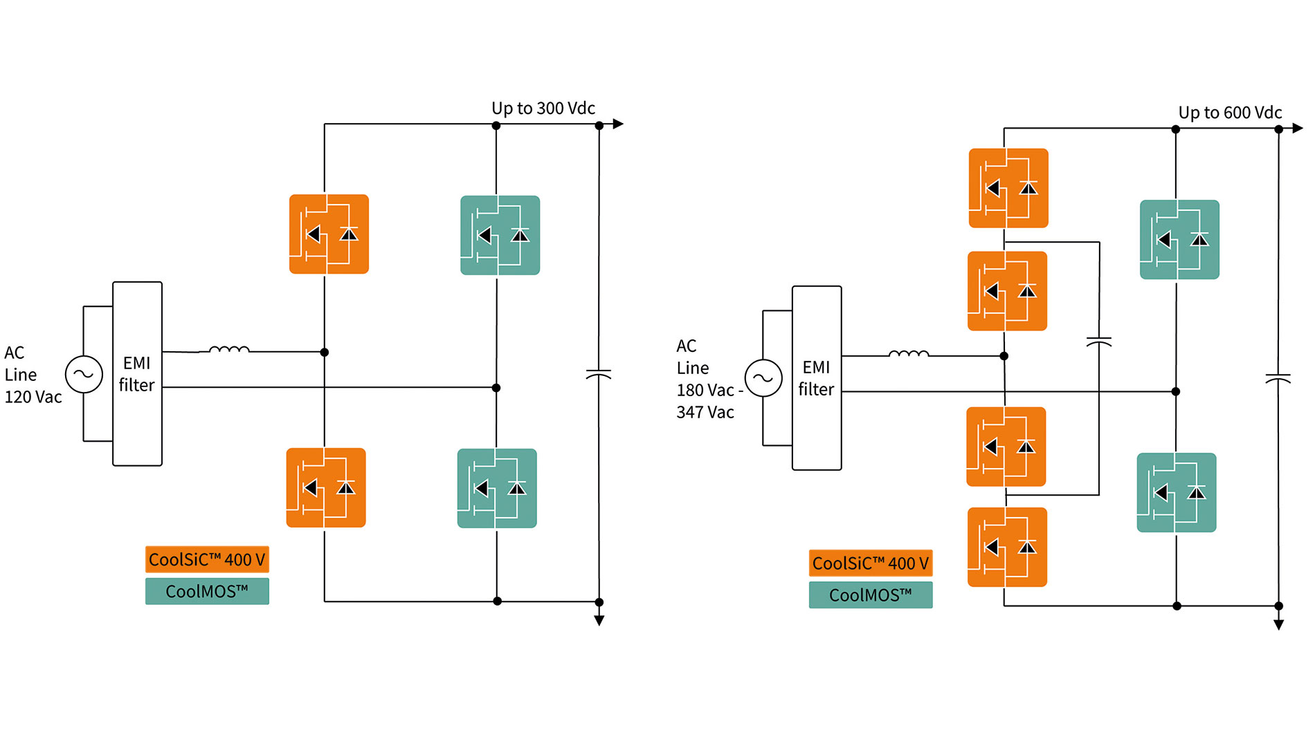
Optimized for 2-level topologies with 120 V (AC) input voltage or up to 300 V (DC) input voltage, and 3-level topologies with 230 to 350 V (AC) or 400 to 600 V (DC) input voltages, CoolSiC MOSFETs 400 V G2 deliver significant gains in switching figures-of-merit (FoMs) and RDS(on) stability over junction temperature. This makes them a perfect fit for hard-switching applications, such as bridgeless bidirectional CCM totem pole PFCs (Figure 1), and softswitching applications, like synchronous rectifiers, to achieve the highest possible system efficiency and power density while optimizing the performance-to-cost ratio.
This article delves into the technology behind CoolSiC MOSFETs 400 V G2 and verify the expected efficiencies and power density gains through measurements in a 3-level flying capacitor CCM (continuous conduction mode) totem-pole PFC (power factor correction) technology demonstrator. By comparing the results with those of a common 2-level totem-pole PFC using 650 V SiC MOSFETs, we showcase the benefits of this innovative technology and its potential to transform the industry.
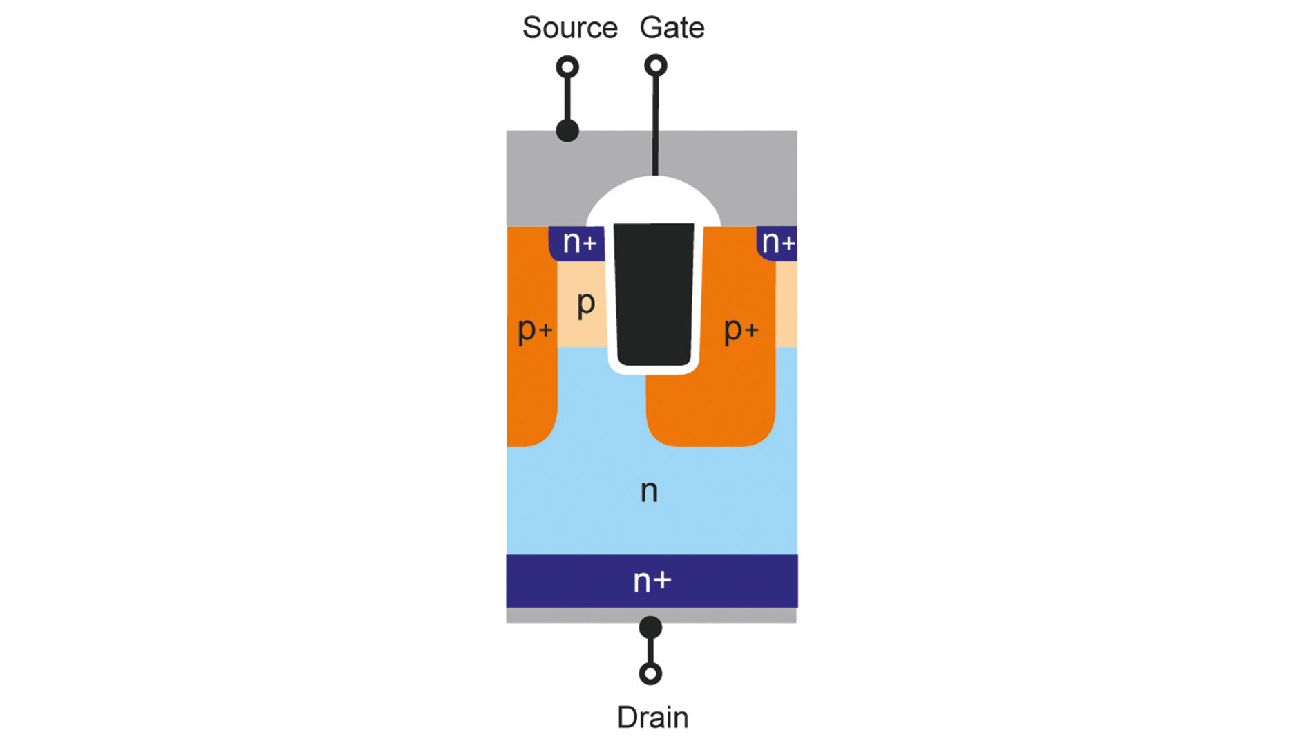
New 400 V SiC trench MOSFET structure for improved performance
Building on the success of first-generation CoolSiC devices, the new 400 V SiC MOSFET takes advantage of continuous technology advancements to deliver even better performance. By reducing the cell pitch and refining channel properties, significant improvements in device performance have been achieved. Moreover, an enhanced control over drift region properties enables more precise management of the device’s behavior. Through meticulous optimization of the chip design, for example the junction termination, the active area loss has been minimized. The result is a next-generation 400 V SiC MOSFET that sets a new standard for performance, reliability, and efficiency, enabling the development of more innovative and sustainable power electronic systems.
Figure 1: Application examples for coolSic 400 V: twolevel and threelevel bidirectional totempole topology, depending on the Ac voltage. Image: Infineon Technologies
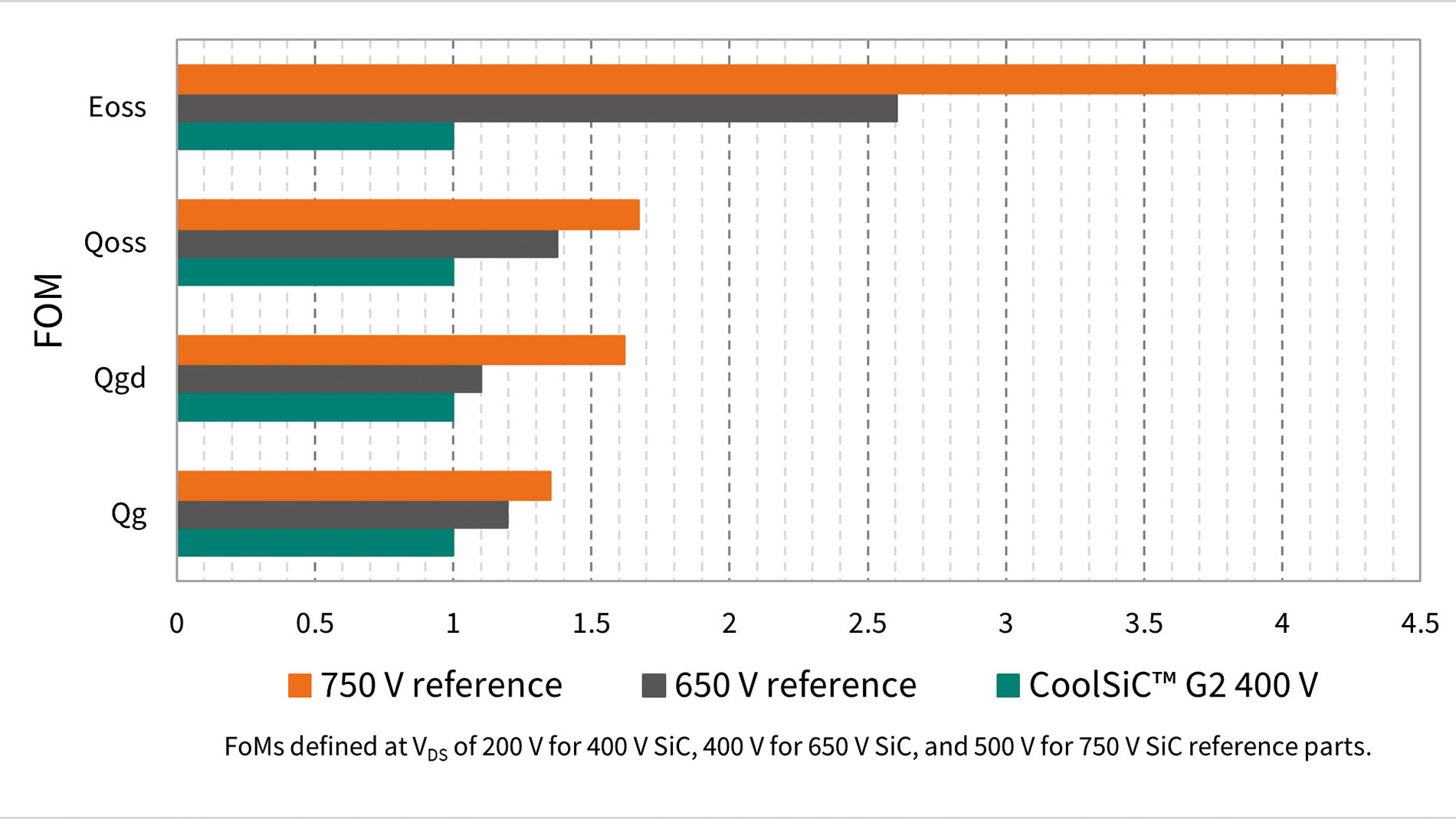
By combining the CoolSiC 400 V with a low-inductance package like TO-Leadless (TOLL), designers can create optimized PCB (printed circuit board) layouts that fully leverage the device’s exceptional switching performance. The high Coss linearity and commutation-robust body diode with low Qfr work together to minimize VDS overshoots and ringing, ensuring stable switching waveforms that are virtually independent of operating temperature and load current. The excellent switching FoMs translate to high switching speeds resulting in minimized switching and dead-time losses, which result in improvement in effciency and power density with good EMI (electromagnetic interference) performance.
Putting CoolSiC 400 V to the test: Performance evaluation in a totem-pole Power Factor Correction
The bridgeless 2-level (2L) totem-pole PFC topology is the state-of-the-art solution for high-efficiency and high power-density designs, eliminating diode-related losses and offering good performance, with efficiencies reaching up to 99 percent. This versatile topology can be operated in various control modes, including continuous current mode (CCM), discontinuous current mode (DCM), critical current mode (CrCM), and triangular current mode (TCM), and is inherently capable of bidirectional power flow. However, to take effciency and power density to the next level in systems with input voltages ranging from 180 to 350 V (AC), multi-level topologies are the way forward. One promising approach to further boost power density is the 3-level (3L) flying capacitor CCM totem-pole topology, as illustrated in Figure 1.
By connecting two devices in series in the high-frequency (HF) leg, for the same DC output voltage, the blocking voltage requirement for each device is halved, resulting in significantly reduced switching losses. Additionally, the voltage swing across the inductor is also halved. When combined with the benefits of “series interleaving” inherent to the flying capacitor topology, the effective switching frequency is doubled compared to the device switching frequency. The higher effective switching frequency combined with a lower voltage swing across the inductor allows for a significant reduction (1/4) in the boost inductance at the same current ripple. For high power rated converters ≥3 kW, the CCM mode of operation in 3L flying capacitor topology enables lower switching losses, lower RMS current related conduction losses, and easier control and EMI filter design due to fixed frequency operation. The combination with an interleaved approach opens the door to an even higher power density. The challenges with the design of 3L flying capacitor topology include – startup, pre-charging and balancing of the flying capacitor under different operation conditions and implementing a robust gate-drive for the floating HF leg MOSFETs. These challenges have been addressed in an upcoming 3.3 kW 3L-flying capacitor PFC reference design from Infineon but have also been investigated widely in the literature due to the significant benefits offered by the topology. Infineon is also positioning the system-solution as a cost-competitive high-performance alternative to the traditional 2-level-CCM totem pole topology for the highest efficiency and power density in the AC/DC PFC stage.
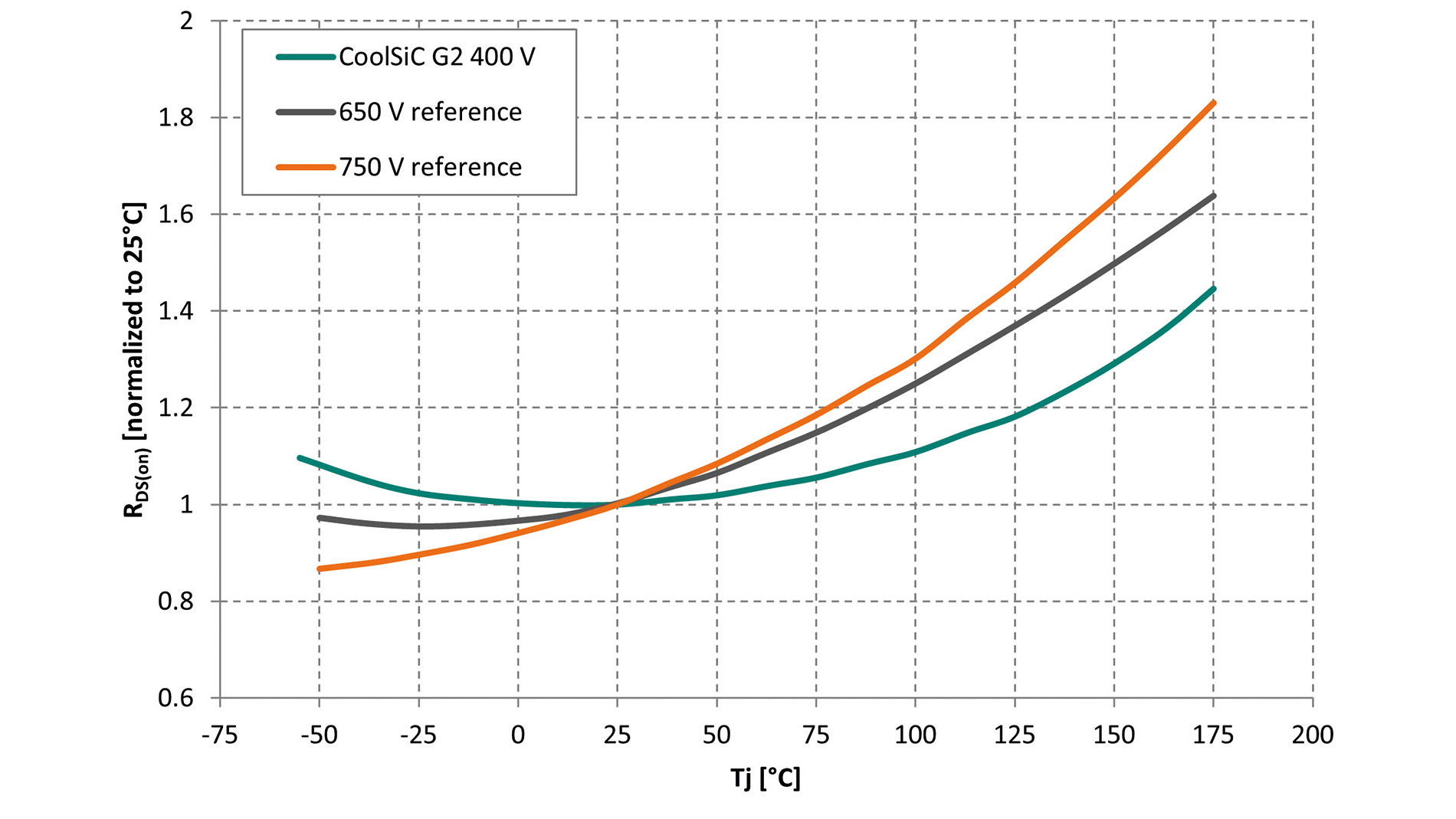
Figure 2: CoolSiC 400 V G2 trench MOSFET structure resulting in improved switching FoMs and stable RDS(on) dependence on junction temperature.
A technology demonstrator for the 3L flying capacitor topology, capable of up to 5.6 kW, was built and is shown in Figure 3. Two interleaved 3-level flying capacitor boost PFC legs are seen in the front. The empty area in the back is reserved for an LLC DC/DC converter for down-conversion to 48 V. With each individual MOSFET in HF PFC leg switching at 80 kHz, the effective switching frequency of a single 3L boost stage is 160 kHz. To further raise the effective frequency seen by the EMI filter, a second interleaved stage is used for an effective frequency of 320 kHz. A hold-up extension circuit (not shown) allows the utilization of more energy out of the DC-link, thus reducing its size. The inductor with an inductance of 50 µH is realized with a RM12LP ferrite core and optimized using litz wire. The power stage uses 400 V, 45 mΩ IMT40R045M2H SiC MOSFETs. Switching frequency and inducto size can be further tuned for higher peak-efficiency or power-density, e. g. by operating the full system well above 400 kHz (>100 kHz per device).
Image: Infineon Technologies
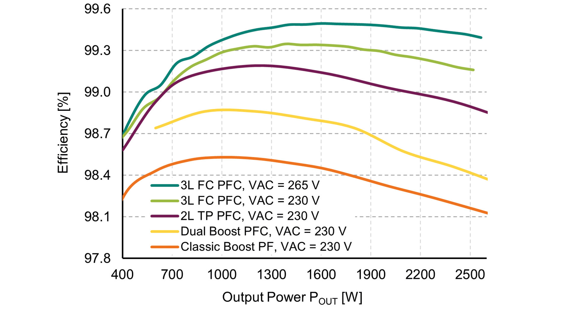
The results presented here use only one of the two interleaved boost stages to facilitate a comparison with the common 2L 3.3 kW totem-pole (TP) PFC that uses 650 V SiC trench MOSFET, as well as with a Classic or Dual Boost PFC employing SJ devices. For the efficiency comparison presented in Figure 4, the 3L FC TP PFC uses CoolSiC MOSFETs 400 V G2, 2L TP PFC uses CoolSiC MOSFETs 650 V G2, while the Dual Boost PFC uses CoolMOS P7, and the Classic Boost PFC uses CoolMOS CFD7A devices. The 3L FC TP PFC outperforms the 2L TP PFC at an AC input voltage of 230 V while operating close to 2.5x the switching frequency. The difference in efficiency at 2.5 kW is substantial: 99.15 percent vs. 98.9 percent, which translates to over 25 percent fewer losses in power conversion. This means significantly lower cooling efforts, making it an attractive solution for data centers and other applications where energy efficiency is key. What’s more, the peak efficiency improves from 99.19 percent for the 2L TP PFC to 99.35 percent with the 3L FC TP PFC.
Image: Infineon Technologies
With the series connection of two 400 V devices, giving a theoretical blocking voltage of 800 V, even higher voltages can be addressed easily. Especially considering the increased power demand of AI in data centers, AC input voltage levels of 277 V (AC) or even up to 350 V (AC) are under evaluation. As can be seen from Figure 4, an increase in the AC input voltage level is also beneficial for the efficiency. In case of 265 V (AC), the peak efficiency further increases to a peak value of nearly 99.5 percent and full load efficiency of 99.35 percent.
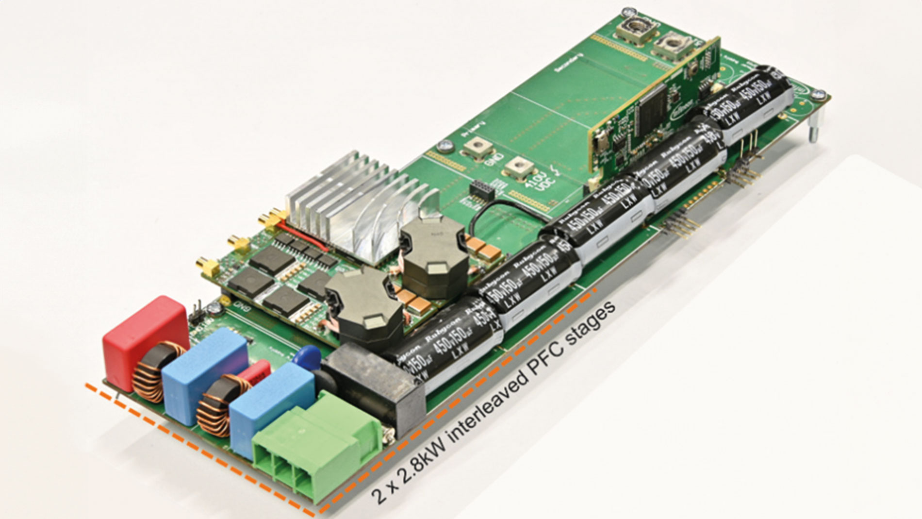
Figure 3: Technology demonstrator platform: Physical PSU mainboard (270 x 83 mm2, 22 mm height) with 2x interleaved 3-level flying capacitor HF legs for PFC, which are 32 x 60 mm2 in size. Image: Infineon Technologies
Conclusions and outlook
The latest CoolSiC MOSFETs 400 V G2 from Infineon offer lower on-state resistances and better Figures-of-Merit over existing solutions, and benefit from a flat temperature dependence of the on-resistance. Low gate-, gate-drain, output- and reverse-recovery charges provide a highly controllable fast-switching capability.
The device performance has been investigated in an ultra-high power density PFC targeting next generation AI server and telecom power supplies. The measurements reveal that the device behaves well even at high switching speeds of 100 V/ns and above. The losses in the investigated PFC design are well-balanced across the different components. The achieved efficiency reaches close to 99.5 percent, with a calculated power density of 140 W/in3. Such power supply units pave the way to next generation AI server and industrial switched-mode power supplies (SMPS), capable of offering scalable solutions to deliver an output power of 5.5 to 8 kW and beyond.
Other application fields enabled by these new 400 V devices include solar and motor-control inverters employing a 3L ANPC inverter topology, or battery-connected drives for light electric vehicles, which could benefit from a higher battery input voltage of 288 V (achieved by a serial instead of parallel connection) using a simple B6 topology, MPPT buck-boost stage of a PV inverter, Class-D audio amplifiers, among many others.
Figure 4: Effciency comparison between the 3L FC TP PFC using 400 V SiC MOSFETs, a 2L TP PFC using 650 V SiC MOSFETs and a classic and dual boost PFC employing 650 V SJ MOSFETs (with applied line filter in the power analyzer). Image: Infineon Technologies