Search and find – our supplier directory provides a comprehensive overview of industry players, featuring detailed profiles of the PCIM Expo exhibitors 2025 as well as the latest solutions and products in power electronics.
Electromagnetic Near-Field Scanning
Description
Fast Facts
- Measurement frequencies from kHz up to 90 GHz
- Two-channel vector signal analyzer for amplitude and phase measurement of the near-field
- Changeable near-field probes for each field component
- Positioning volume of 50 cm x 80 cm x 50 cm
- Positioning accuracy of 1 µm
- 3D scanning unit for an automatic and collision free measurement procedure
- Measurement of (micro-)magnets
- Measurement as a service and development of customized scanning tools
The More-than-Moore assembly trend of electronic systems makes components continuously smaller, integrating heterogeneous functionalities with smaller switching times. In parallel, the signal-to-noise-ratio decreases, making circuits more sensitive. This results in increasing electromagnetic compatibility (EMC) issues.
By using appropriate EDA tools and simulators, it is possible to analyze a multitude of such parameters in the design phase. However, due to the complexity of modern systems and size differences of their components, the resulting 3D models become extremely complex or even unfeasible. Nevertheless, it is essential to consider that the radiating characteristics are directly determined by the circuit‘s switching behavior and its geometric structure.
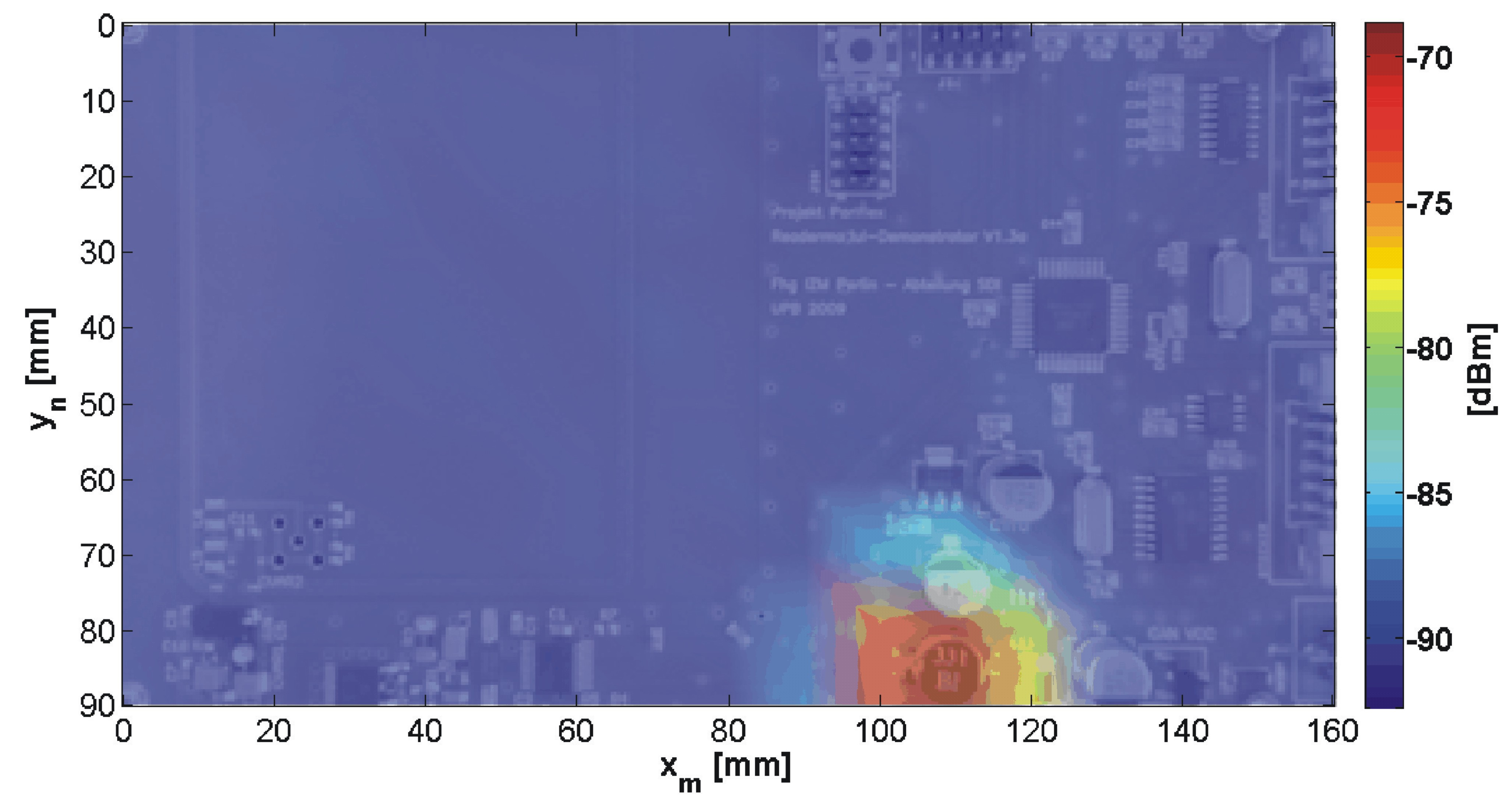
Near-field measurement techniques using the NFS3000 provide a mitigation to this problem. It allows the precise detection of weak electric and magnetic fields in the frequency and spatial domain within a resolution of a hundredth of a millimeter. This becomes possible because of the optical height scan of the system‘s surface that is used. This precise near-field measurement can be employed for the characterization and discrimination of potential electromagnetic interferences (EMI) sources in active systems.
Thanks to these properties, it is possible to quickly and directly identify and correct conception faults at early design stages. By using near-field measurements and the NFS3000, it is possible to uncover electromagnetic weaknesses in systems such as EMC/EMI issues, malfunctions or security-related aspects. Using the measurement results, countermeasure strategies can be elaborated without trial-and-error approaches.
Optimized System Design by Near-Field Measurements
- Accompaniment early in the system design phase
- Visualization of electric and magnetic field distribution in magnitude and phase
- Combination of near-field measurements with 3D full-wave simulations through equivalent near-field sources
- Near-field to far-field transformation
- Estimation of the far-field radiation without measuring in an anechoic chamber
- EMC-compliant system design
- Security and functional analysis
Fields of Application
- PCB design and production
- Chip industry
- Communication electronics and radio technology
- Entertainment electronics
- Aerospace
- Power electronics
- Wireless power transmission
- EMC test laboratories / test centers
- RF systems and antennas
- 5G and radar applications
- (Industrial) Internet of Things
You can find us here:

Address
Fraunhofer-Institut für Elektronische Nanosysteme ENAS
Technologie-Campus 3
09126 Chemnitz
Germany
Telephone+49 371 450010
Discover more from us