Dr. Martin Wattenberg, Dr. Matthias J. Kasper, Dr. Ralf Siemieniec
I. INTRODUCTION
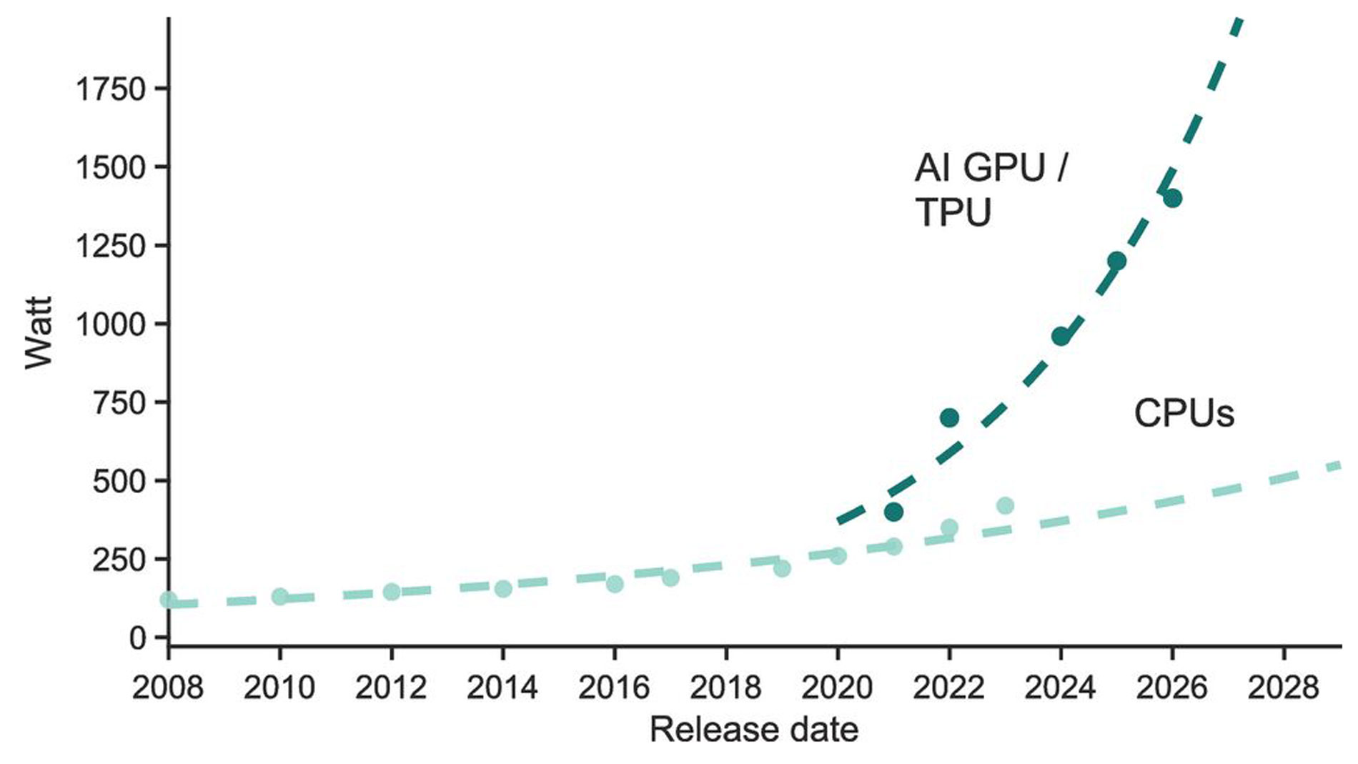
Data centers have historically experienced increasing power demands, primarily driven by CPU power consumption. However, the advent of large language models (LLMs) and the associated use of GPUs/TPUs have significantly accelerated this trend. These processors, with their numerous compute cores, consume substantially more power than traditional CPUs, and their power requirements increase with each generation, as shown in Fig. 1.
As a result, also the power consumption of AI compute racks is continuously increasing from 60-70kW compute racks to advanced AI solutions exceeding 132 kW+ per rack. Plans for rack power at the scale of 500 kW and above are beginning to appear on the horizon.
To address these increasing power demands, hyperscale data centers are adopting new datacenter architectures, such as placing power supply units (PSUs) in multiple power shelves, e.g., at the top or bottom of racks, as proposed by the Open Compute Project.
Experts
Dr. Martin Wattenberg is responsible as a System Application Engineer for the development of innovative systems using WBG switches.
Dr. Matthias Kasper is leading Infineon’s innovation group for upcoming trends in the area of data centers, on-board charging, and optimized power conversion.
Dr. Ralf Siemieniec is a semi-conductor device specialist and developed several key technology concepts for silicon and silicon carbide MOSFETs.
These power shelves typically house six PSUs in a 5+1 redundancy configuration. Single-phase PSU power ratings have quickly increased from 3.3 kW to 5.5 kW, with 8 kW units being deployed. This article presents a 12 kW PSU designed to meet the demands of even higher rack power levels.
In addition to the significantly increased power level and limited space, load transients are another key challenge for AI data centers with synchronized GPU clusters. The power demand of GPUs can surge from 0 percent to 200 percent load for 500 µs during training batch initialization before receding to 100 percent. These load steps, occurring every 1-2 s, can create sub-harmonics on the power grid and increase electricity costs [1]. While super-capacitor shelves can mitigate these issues, they consume valuable space. The power pulsation buffer presented in this article offers an attractive solution by utilizing the DC-link capacitors already present in the PSU more effectively.
Another challenge is the thermal budget and limitations of air-cooling. While GPUs are increasingly liquid-cooled, PSUs remain primarily air-cooled, often relying on a single 40mm fan. Due to the growing length of the PSU, back pressure increases and makes heat extraction more challenging. Component placement must balance airflow and power density.
II. SYSTEM CONCEPT
To optimize efficiency, power density, and thermal design, the 12 kW PSU consists of two stacked 6 kW units, each below 1/2 U height. This modular approach broadens component selection, especially for the input relay, and also enables the use of lower-rated fuses, which typically have a shorter clearing time. Crucially it provides twice the surface area and components can be spread out over two PCBs further reducing hotspots.
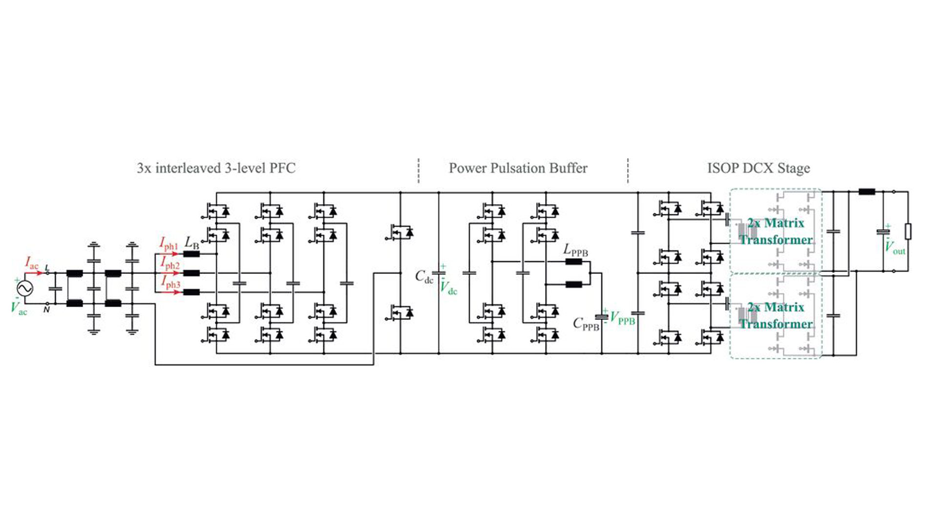
The topology of each 6 kW unit, shown in Fig. 2, includes a PFC, a power pulsation buffer, and a DC/DC stage.
Fig. 2: Schematic overview showing the topology used in the 12 kW demonstrator: Totem-pole PFC with 3x interleaved 3-level flying capacitor bridge legs, power pulsation buffer with 2x interleaved 3-level flying capacitor bridge legs, and unregulated DCX converters in ISOP configuration
1) PFC stage: A three-times interleaved, three-level flying capacitor totem-pole PFC topology reduces magnetics size and maximizes efficiency. The flying capacitor bridge-leg introduces a third voltage level and doubles the effective switching frequency, reducing the voltage time-area seen by the boost inductors. Parallel interleaving three flying capacitor bridge-legs reduces current stress on inductors and semiconductors, enabling low-profile inductors. It also boosts the effective switching frequency seen by the EMI filter, allowing for a smaller EMI filter. The series and parallel interleaving also creates a heat-spreading effect, preventing hot-spots. The MOSFETs are operated at 80 kHz on device level, resulting in 160 kHz of current ripple on the inductors. Due to the interleaving of three phases, an effective switching frequency of 480 kHz towards the EMI filter was achieved.
2) Power Pulsation Buffer (PPB): To ensure server uptime during line-cycle dropouts (LCDO), PSUs must provide full power (12 kW) for at least 20 ms, requiring 240 J of stored energy. A power pulsation buffer decouples the energy storage capacitors from the DC-link, allowing them to discharge to half their voltage during LCDO, extracting 75 percent of their stored energy and reducing capacitor size.
The PPB also compensates for the twice line-frequency power pulsation from the input and also ensures a stable DC-link voltage during load jumps. The PPB also takes advantage of interleaved three-level flying capacitor bridge legs with lower inductance for faster transients and wider control bandwidth
3) DC/DC Stage: The pre-regulation of the DC-link voltage by the PPB allows for an unregulated DC/DC converter stage. Two series resonant converters (DCXs) operating at the resonant frequency, connected in an input-series output-parallel configuration with matrix transformers, offer several advantages:
- Load-independent soft-switching.
- Resonant current with low harmonic content, minimizing AC losses.
- Reduced component count compared to LLCs.
- Self-balancing of the stacked input capacitors [2].
The DC/DC stage’s step-down ratio is set at 10:1, resulting in a DC-link voltage of VDC = 500V for an output voltage of Vout = 50V.
Since all high-frequency devices in this system are exposed to only half the DC-link voltage (250 V), Infineon’s 400 V CoolSiC MOSFETs are a great match in this application.
A. 400 V Silicon Carbide MOSFETs
The 400 V CoolSiC MOSFETs offer improved performance and efficiency compared to existing solutions. They feature small gate, output, and reverse-recovery charges, and a linear output and Miller capacitance over drain voltage [3].
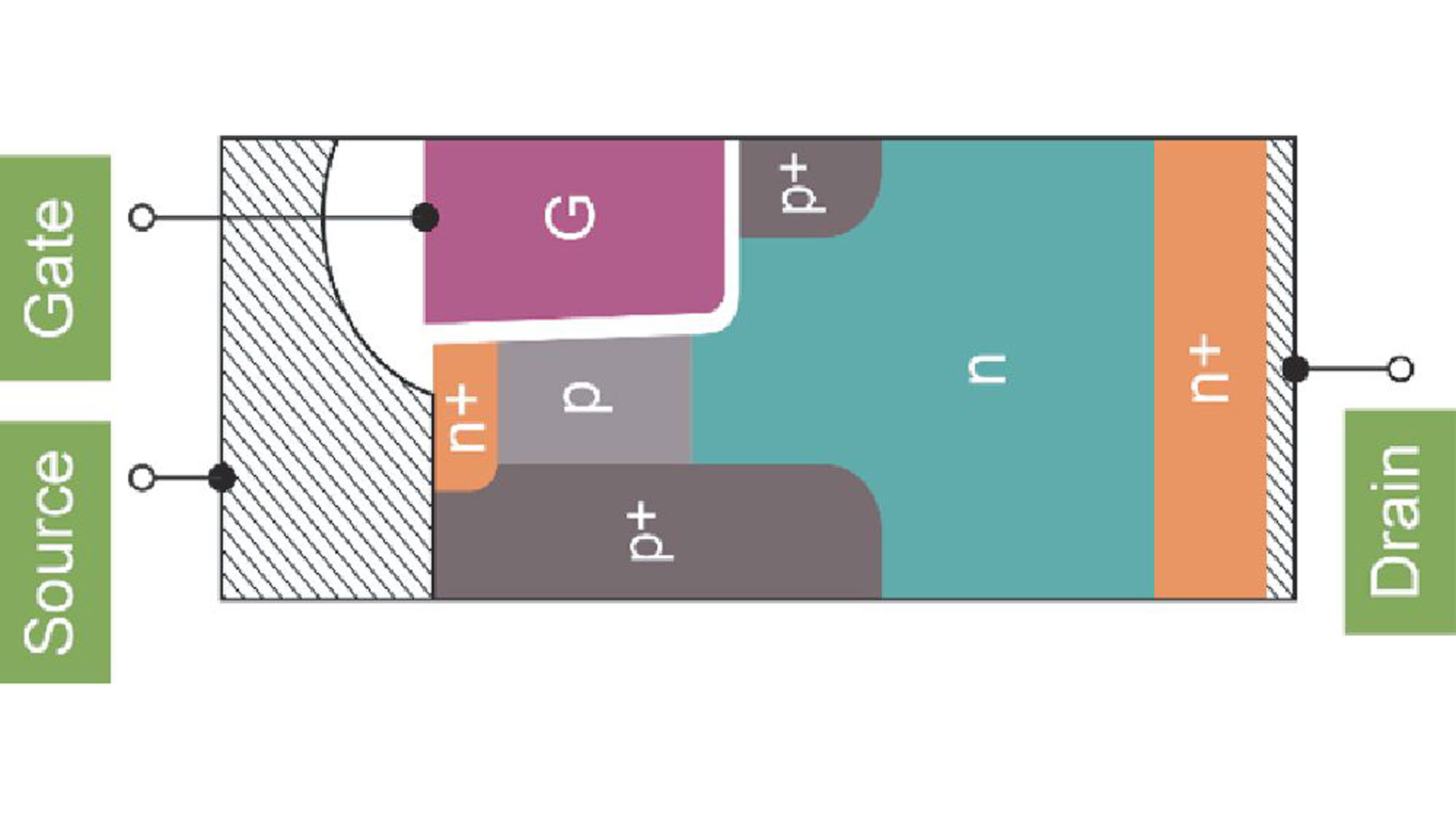
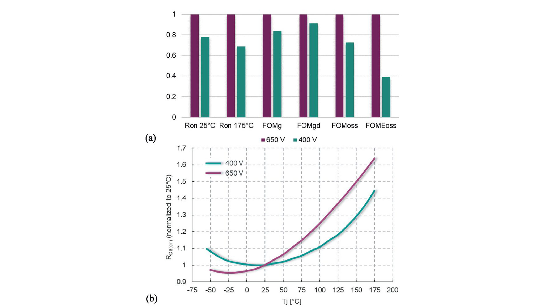
The device structure builds upon previous designs [4], [5]. Fig. 3 shows the cell concept. The active channel aligns along the a-plane for optimal channel mobility. Deep p-wells protect the gate oxide. The new 400 V MOSFET benefits from continuous technological advancements. Fig. 4(a) compares key device parameters between the new 400 V and 650 V CoolSiC technology. The temperature dependence of on-resistance increases by 11 percent from 25 °C to 100 °C, whereas for a 650 V SiC MOSFET it increases by 25 percent, as shown in Fig. 4(b).
III. THERMAL MANAGEMENT
Thermal management is critical in high power-density PSUs as heat degrades electrical performance and shortens component lifespan.
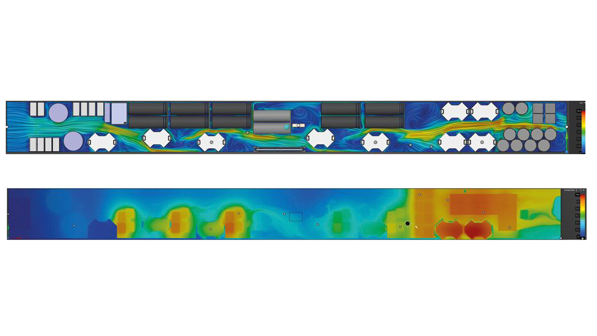
Based on a virtual design, thermal and CFD calculations, shown in Fig. 5, were performed. The air intake is on the left, while the outlet and connector are on the right. Components were strategically placed to minimize obstruction while directing airflow over heat-generating components.
Assuming a conservative full-load efficiency of around 97 percent, a total of 360 to 400 W of heat needs to be evacuated. Using state-of-the-art server fans, a realistic airflow target for the given length of 720 mm of the supply is 15 to 20 CFM. This corresponds to a maximum acceptable back pressure of 700 to 900 Pa for the strongest fans available. If back-pressure is too low, heat transfer can be improved with increased surface area. Conversely, excessive back-pressure restricts airflow. The chosen operating point resides just outside the stall region of the fan before airflow significantly drops. Therefore, component spacing and airflow channel design can significantly impact temperature, efficiency, and component lifespan.
IV. HARDWARE DEMONSTRATOR
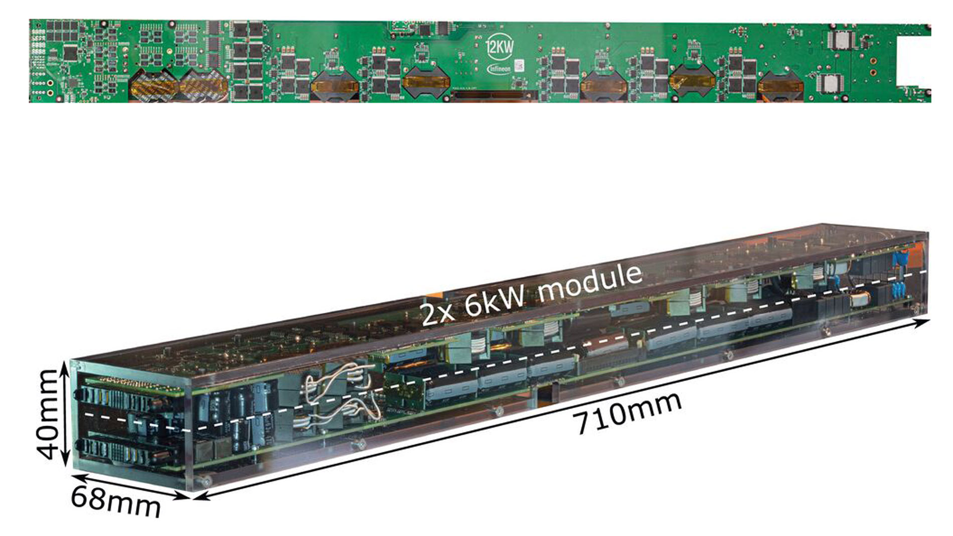
A hardware demonstrator was built and is shown in Fig. 6. Components were Pareto-optimized to achieve maximum efficiency within the height constraints of each 6 kW module. This height constraint influenced the selection of core sizes for magnetic components and capacitor sizes. Remaining degrees of freedom included winding configurations, switching frequencies, and semiconductor chip sizes.
Thanks to the large portfolio of 400 V CoolSiC MOSFETs, an optimal RDS,on could be chosen for each part of the circuit: 35 mΩ for the PFC stage, 25 mΩ for the PPB, and 15 mΩ for the primary side DCX. The secondary side DCX uses the recently introduced CoolGaN 80 V SG HEMT with 2.5 mΩ and two devices per switch in parallel.
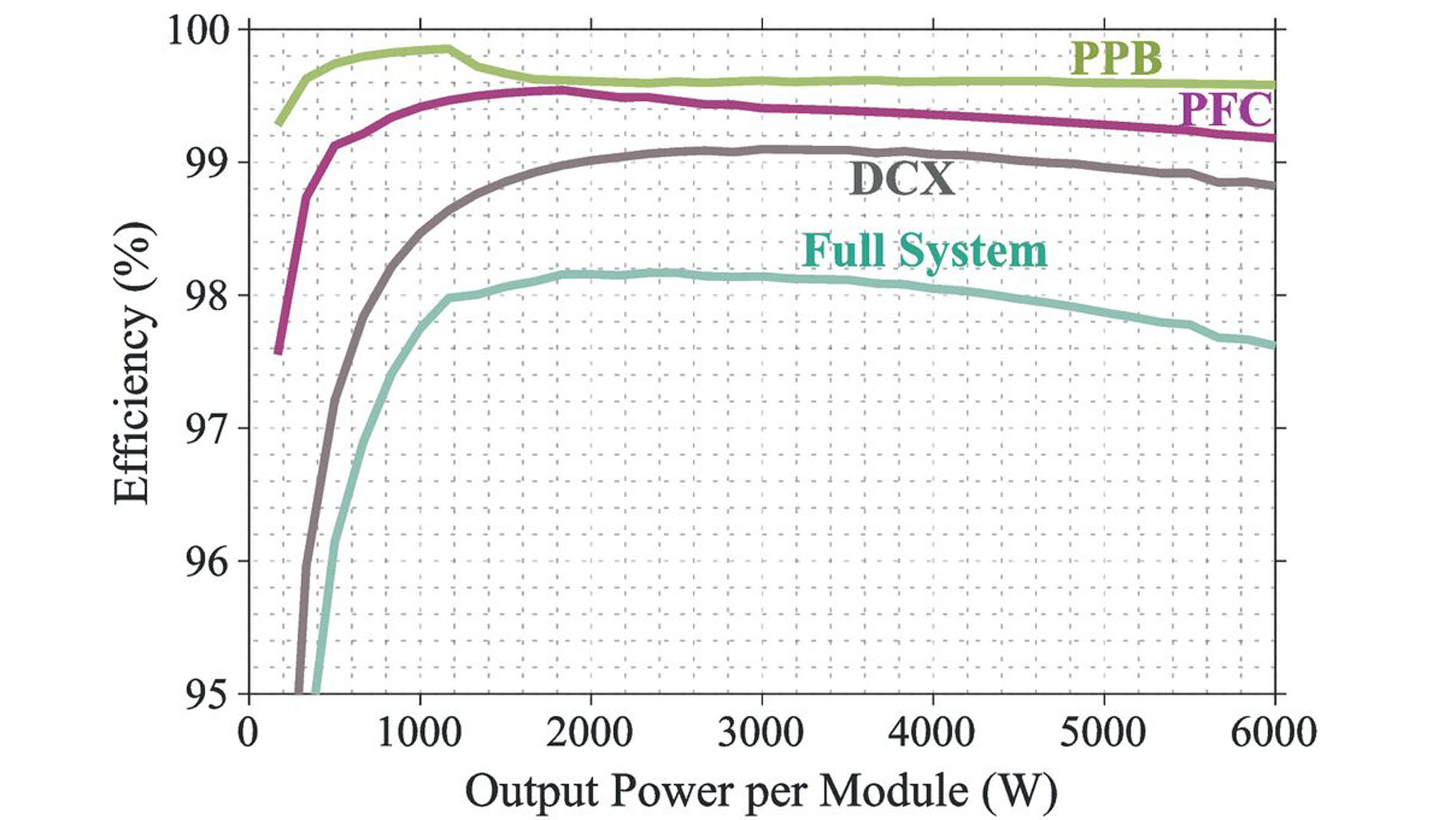
The calculated efficiency of the entire PSU and its individual stages at Vin,rms = 277 V are shown in Fig. 7.
The system is controlled by the recently released Infineon PSOC Control C3 Main Line MCU. Due to the high number of complementary PWM channels available (20 in total), all primary and secondary switches can be controlled from one centralized MCU. This simplifies firmware development, avoids latency from inter-MCU communications, and reduces layout complexity. No secondary-side sync. rec. controllers are needed, as the DCX operates in resonance with no phase shift between the primary and secondary sides. This enables fine-tuning of switching patterns to minimize deadtime losses. Propagation delays are closely matched using the same coreless transformer (CT) isolation technology on all signals.
A smaller secondary-side MCU (PSOC C3 Entry Line) relays output voltage and current information to the primary side across the isolation barrier via the Infineon ISOFACE Digital Isolators. This MCU could also interface with the PMbus, providing necessary information to the rack controller.
V. EXPERIMENTAL RESULTS
Preliminary tests have been conducted to validate the proposed control concept by running the converter at reduced power and voltage levels. The waveforms presented here demonstrate the practical feasibility.
The waveforms at the top of Fig. 8 show one of the PFC inductor currents (teal), along with the respective switch-node (green), and AC input voltage (red). What is noteworthy here is the constant voltage levels seen on the switch node. Typically, this would exhibit a ripple of twice the line frequency, but due to the operation of the PPB, the voltage is near constant.
The center of Fig. 8 shows the two inductor currents (blue and teal) of the PPB, which run at twice the line frequency, and the switch node voltage of the PPB (orange). It can be nicely seen how the PPB provides peak positive current during zero-crossing of the input voltage and absorbs the same amount during peak line voltage.
The bottom of Fig. 8 presents the differential output voltages of each stacked DCX stage, along with the primary-side transformer current. The combined output current on the secondary side reached 40 A. Full ZVS transition was achieved with a deadtime of 100 ns. The transformers used were hand-wound prototypes, exhibiting some variation in stray and main inductance and thus slight differences in currents.
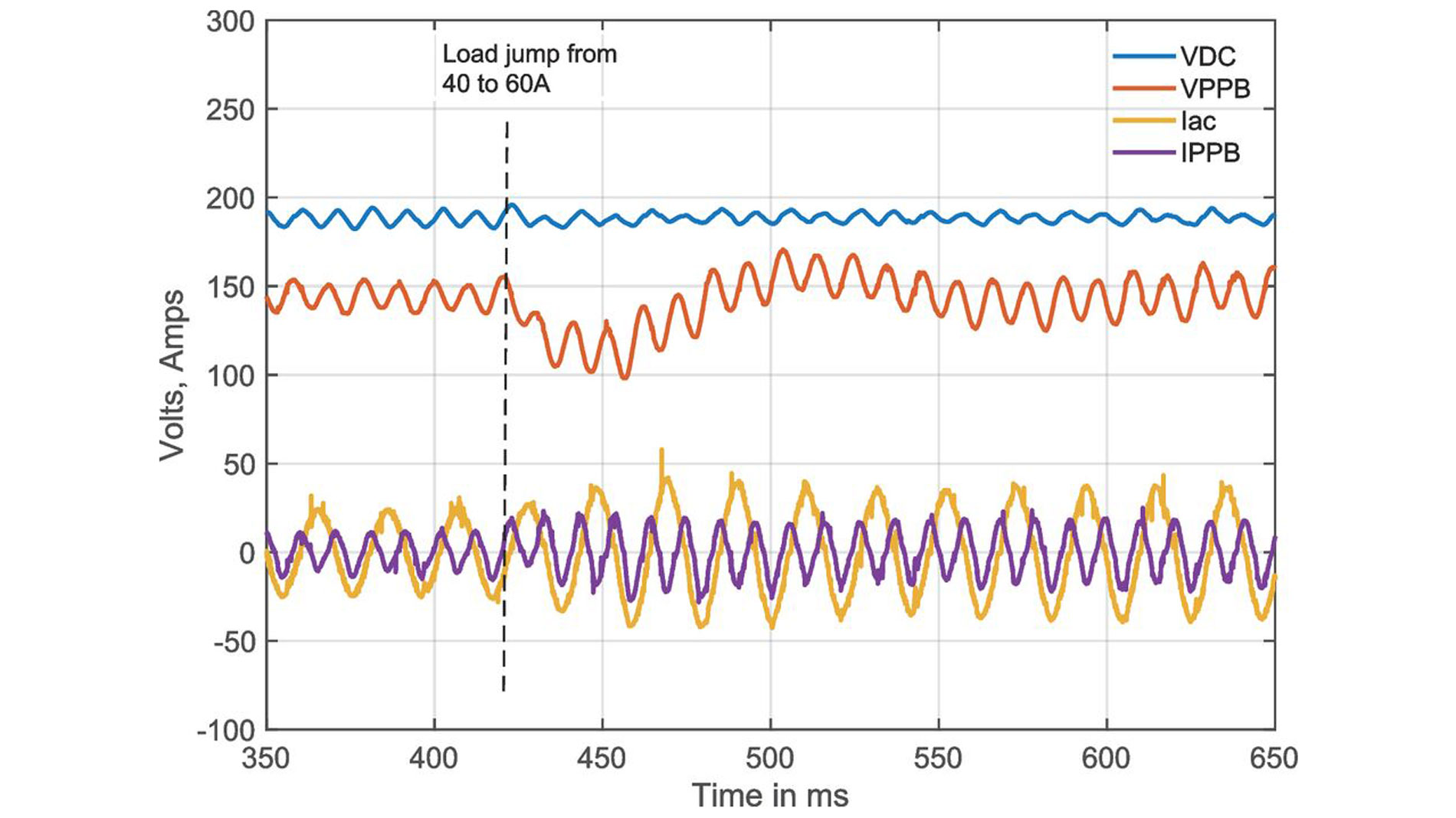
Fig. 9 shows a transient load jump for 40 to 60 A output current. It can be clearly seen that the DC-link voltage remains constant while the voltage on the PPB drops temporarily. Additionally, the AC input current does not show any discontinuities and instead smoothly ramps up the input current until a new steady state is reached. Some minor ripple can be observed on the DC-link voltage caused by a non-optimal control parameter set in this early implementation.
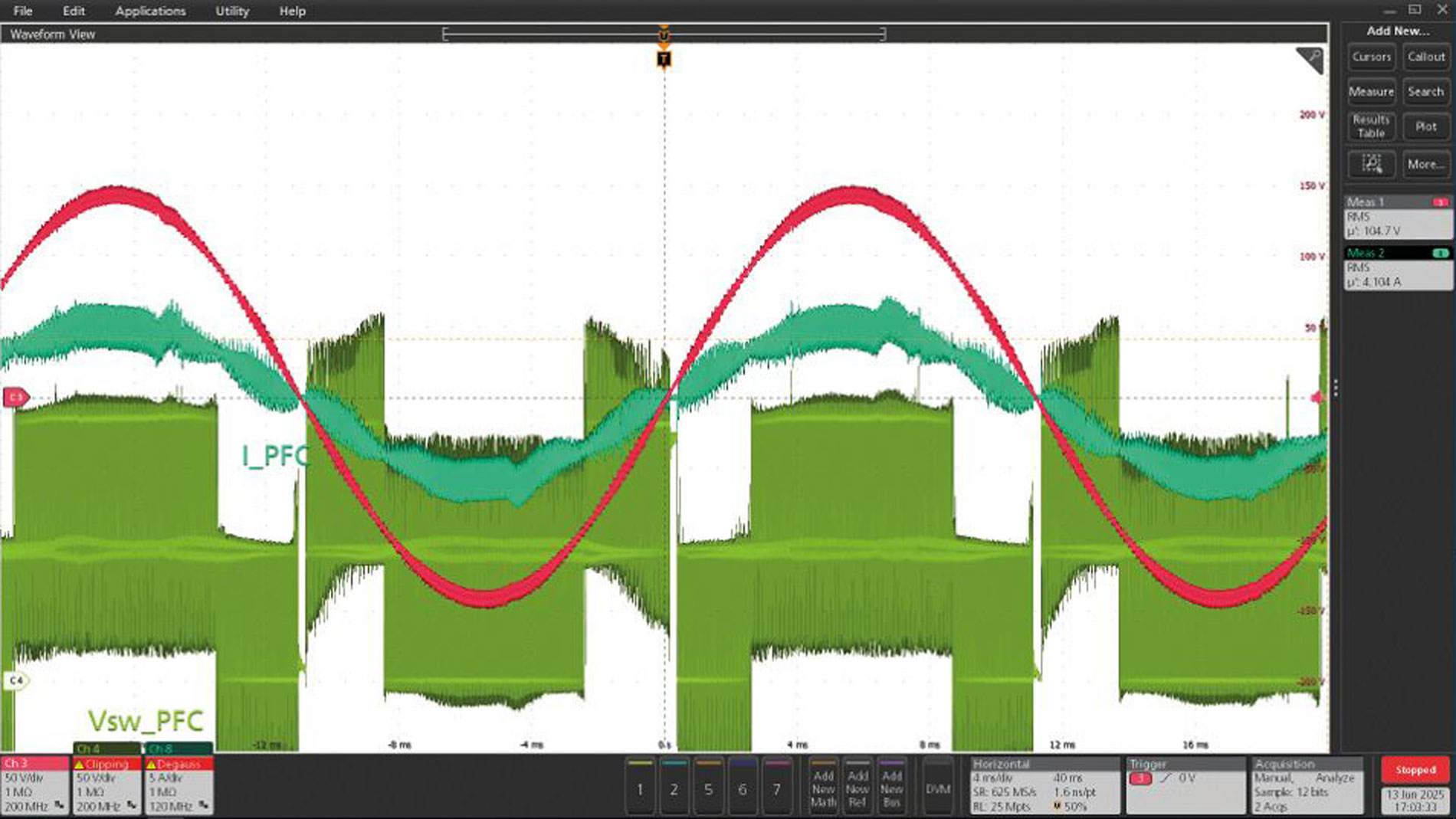
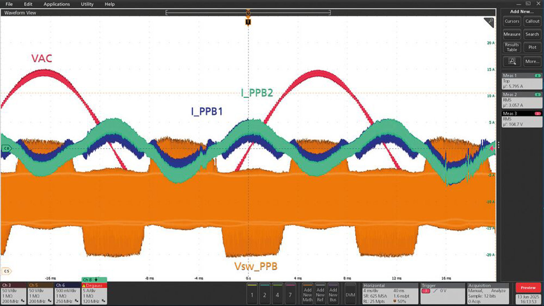
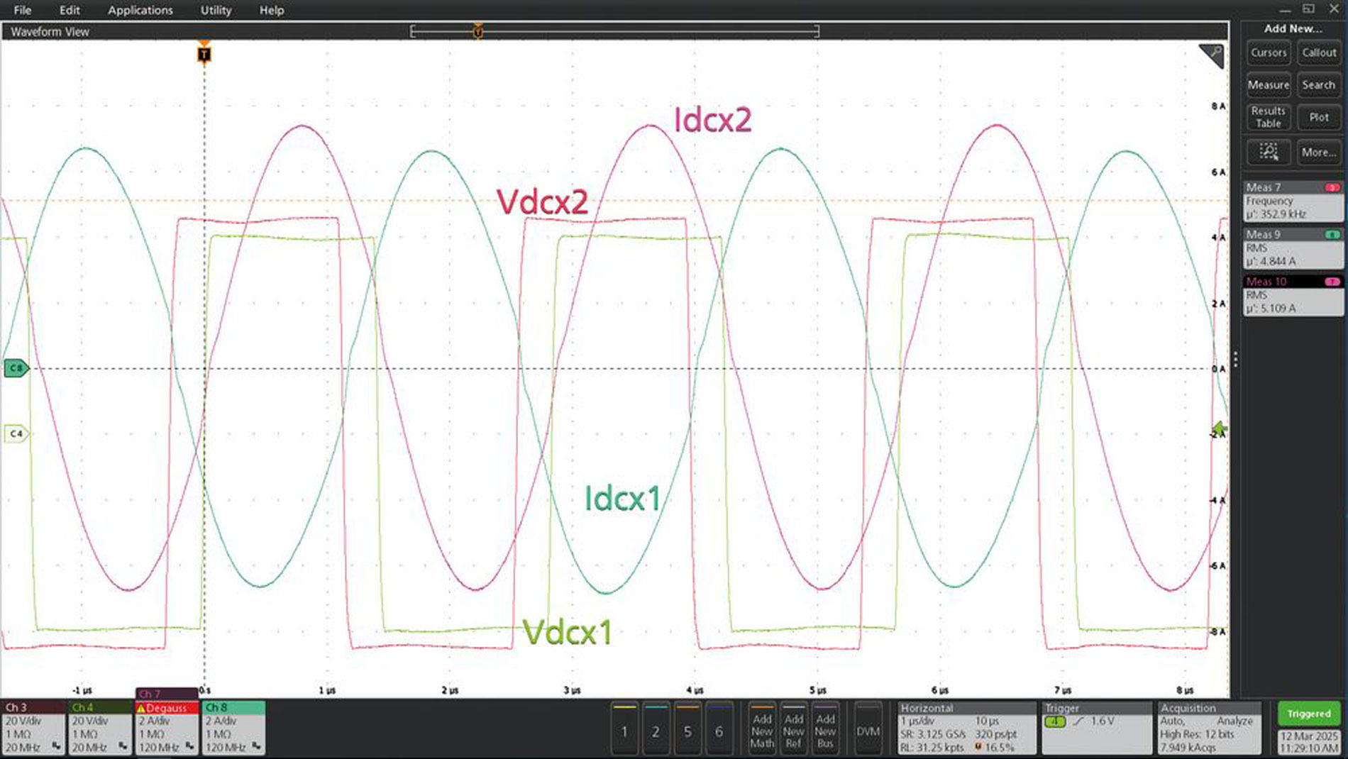
Fig. 8: Preliminary measurement results. Top: PFC input current with active PPB. Center: PPB currents in sync. With line frequency. Bottom: stacked DCX voltage and current
VI. CONCLUSION AND OUTLOOK
The increasing power demands of AI, driven by large language models, present significant challenges for data centers. Innovative solutions are needed across the entire power conversion chain.
Future AC/DC server power supplies will exceed the 5.5 kW specified by the Open Compute Project. An attractive solution for these challenges are multi-level topologies. They are key to achieving efficiency and power density within the 1 U (40 mm) height constraint. Infineon’s 400 V CoolSiC MOSFETs are an excellent choice for these topologies.
The power pulsation buffer concept presented in this article leverages the already existing DC-link capacitors and offers several key advantages. On the one hand, the bulk capacitance for complying with hold-up time requirements can be reduced. On the other hand, by maintaining a fixed DC-link voltage, an unregulated DC/DC stage (DCX) with higher efficiency and power density than a classic LLC can be used. Additionally, the impact on the upstream grid due to load transients can be significantly. Lastly, in case of a line-cycle drop out, the power pulsation buffer maintains a constant DC-link voltage above peak line voltage and thus avoids re-rush current into the PFC.
Thermal management, constrained by the limited heat extraction capability of a single fan, presents a design challenge. Splitting the system into two stacked 6 kW units improves heat spreading and surface area.
This 12 kW power supply enables rack power levels up to 240 kW. At this power level, the 48 V bus bars will reach their limits, potentially leading to 3-phase power supplies with high-voltage power distribution. eg
Fig. 9: Transient load jump from 40 to 60 A showing the effective compensation of via the Power Pulsation Buffer
REFERENCES
[1] M. Dabbagh et al., “Shaving data center power demand peaks through energy storage and workload shifting control,” IEEE Trans. Cloud Computing, vol. 7, no. 4, pp. 1095-1108, 2019.
[2] M. Kasper et al., “Scaling and Balancing of Multi-cell Converters,” in Proc. IPEC, 2014.
[3] R. Siemieniec et al., “New 400V SiC MOSFET and its use in Multi-Level Applications,” in Proc. ECCE Europe, 2024.
[4] D. Peters et al., “The New CoolSiC™ Trench MOSFET Technology for Low Gate Oxide Stress and High Performance,” in Proc. PCIM, 2017.
[5] R. Siemieniec et al., “650 V SiC Trench MOSFET for high-efficiency power supplies,” in Proc. EPE, 2019.