.jpg)
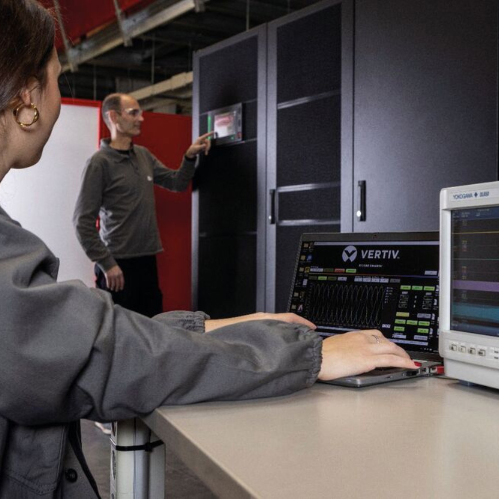
A significant role for GaN today
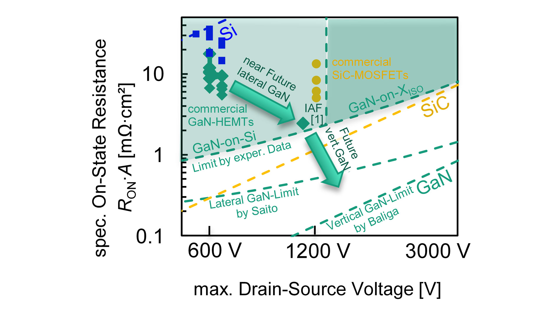
Compared to silicon technologies (Si-MOSFET and Si-IGBTs), silicon carbide (SiC) MOSFETs offer very good efficiency and switching properties. This is why they are being increasingly used in energy transition solutions. But the relatively high substrate costs make SiC MOS-FETs comparatively expensive.
Gallium nitride (GaN) offers an alternative. GaN devices are efficient and fast-switching, and – thanks to processing on large-area (≥ 8”), low-cost Si carrier substrates – cost-effective. This is proven by 10 years of commercial availability, and the frequent use of lateral GaN HEMTs in consumer voltage converter applications.
However, the constrained thicknesses of the GaN layers in GaN-on-Si technology means they are stress-limited, typically up to reverse voltages of 650 V. This means GaN compo-nents are not in consideration for many energy transition applications. However, there is research into higher voltage classes, through the continuous development and optimization of substrate quality, crystal growth layers, pro-cess technology, and device structure.
Insulating substrates to boost voltage classes
Such research has already shown reverse voltages of up to 1200 V are achievable for GaN- on-Si HEMTs. There is also a trend to replace the conductive Si carrier substrates with highly insulating carrier substrates (sapphire, SiC, GaN, ...). Preventing a vertical breakthrough path to the substrate, removes the practical voltage limit for lateral GaN HEMTs on insu-lating carriers. There are commercial products with GaN HEMTs on sapphire that can handle reverse voltages up to 1250 Vi, and voltage classes beyond 1200 V can already be found in the current scientific literature.
GaN-on-sapphire is very interesting for commer-cialization, because the sapphire substrate has already been developed for LED applications on large-area wafers (6”) This should pave the way for attractive pricing, with good material quality. It seems likely that in the next 3 or so years, high-performance, efficient and cost-effective GaN HEMTs on insulating substrates will be available for applications ≥ 1200 V).
Vertical GaN technologies on the horizon
Longer term, the full potential of GaN semiconductors can only be realised with vertical GaN transistors. Currently, GaN wafers for vertical devices have limited availability, for smaller di-ameters (≤ 4”), at significant costs. However, larger diameters, improved material quality, and lower costs are in development.
There is also research on other component technologies (GaN-CAVET, GaN-FinFET, GaN-JFET, GaN-MOSFET, ...). These aim to reduce the on-state resistance relative to the chip area (Ron∙A), to define gate modules suitable for use in products (normally-off, leakage currents, robustness, ...), as well as improving reverse voltage resistance. The next 10 years should see lots of exciting GaN technologies, to enable further leaps in the development of energy transition applications.
i R. Reiner et al.,”More than 1200 V Breakdown and Low Area-Specific On-State Resistances by Progress in Lateral GaN-on-Si and GaN-on-Insulator Technologies”, in Proceedings of the PCIM Europe, 2024.