To put it somewhat provocatively: the world is entering a new era in which energy is significantly limiting technological progress. Or to put it another way: the demand for electricity is growing faster than our ability to generate and deliver it efficiently. The use of vertical GaN power semiconductors could reduce this bottleneck by bringing energy conversion closer to the chip, resulting in less energy loss and heat generation, which could be crucial for the power supplies of the future in computers and AI blades, for example.
Higher operating voltages are associated with faster switching frequencies. In AI and electric car applications, there are many arguments in favour of 1200 V power semiconductors. Until now, this has not been possible with GaN as a single chip. Lateral GaN power semiconductors utilise the conduction properties of two-dimensional electron gas, but due to limited GaN layer thicknesses, the reverse voltage of lateral GaN power semiconductors has been limited to 650 V. Anyone who wanted to use them for higher voltages had to resort to special circuit designs.
It would be much simpler to use just one GaN component with a 1200 V reverse voltage. Because the voltage drops across the entire substrate when switched off, vertical GaN component designs offer significant advantages at higher operating voltages of 1200 V and above. They combine thick epitaxial layers for blocking high voltages in the off state and a very high current density in the on state in a single component. Higher power per chip enables smaller and lighter designs, saving space and material. Vertical GaN components also offer the possibility of better heat dissipation through double-sided cooling, which improves performance and reliability. A vertical chip design also enables easy chip-on-chip integration, which is interesting for applications such as LiDAR, among others.
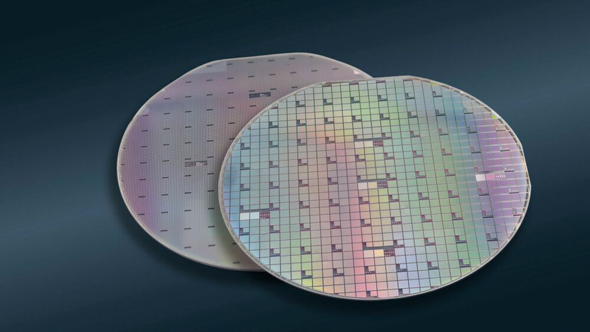
Until recently, it was assumed that vertical GaN in the form of a 1200 V switch would not be available on the market as a series product until the end of this decade, but it now looks as if this could happen sooner. In autumn this year, onsemi presented its vGaN technology, GaN-on-GaN power semiconductors, which are initially to be available with reverse voltages of 700 and 1200 V. onsemi points out that its technology is protected by over 130 global patents covering a range of fundamental process, device design, manufacturing and system innovations.
This means that onsemi has apparently succeeded in transforming NexGen Power Systems’ expertise into a market-ready product much faster than experts had thought possible in December last year. At that time, onsemi acquired the DeWitt plant in Syracuse, New York, and the intellectual property of NexGen Power Systems for $20 million. NexGen had to file for bankruptcy in January 2024. Back in May 2023, onsemi had hired NexGen’s former co-founder Dinesh Ramanathan, who has since served as Senior Vice President of Corporate Strategy at onsemi.
He was also the one who emphasised the significance of onsemi’s product launch: ‘Vertical GaN is a milestone for the industry and solidifies onsemi’s leadership position in energy efficiency and innovation. The addition of vertical GaN to our performance portfolio provides our customers with the ultimate toolkit for unmatched performance. With this breakthrough, onsemi is defining the future, where energy efficiency and power density are the currency of competitiveness.’
The new technology has a wide range of potential applications. For example, it can significantly increase the power density of 800 V DC/DC converters for AI computing systems. In electric vehicles, smaller, lighter and more efficient inverters could enable longer ranges in the future. In the field of renewable energies, vertical GaN would enable higher voltage resistance and lower energy losses for solar and inverters. In energy storage systems (ESS), to give another example, they could provide fast, efficient, bidirectional, high-density energy for battery converters and microgrids.
Unlike other solutions that use silicon or sapphire substrates for their GaN power semiconductor switches, onsemi relies on GaN-on-GaN technology for its vGaN technology. This design offers higher power density, greater thermal stability and robust performance under extreme conditions, outperforming both GaN-on-silicon and GaN-on-sapphire devices. With the introduction of the new technology, onsemi made both 700 V and 1200 V versions of its vGaN chips available to early access customers. It remains to be seen whether a broad market launch will take place as early as 2026.
Even though onsemi is clearly ahead of the game with the introduction of market-ready vertical 1200 V GaN power semiconductors, other companies are also working intensively on similar solutions. One example is Vertical Semiconductor, a company that emerged from the Palacios Group, a GaN research lab at MIT. CEO and co-founder Cynthia Liao makes it clear where she sees the need for vertical GaN: ‘The pace of AI is not only limited by algorithms. The biggest bottleneck in AI hardware is the speed at which we can deliver power to the silicon chip. With vertical GaN, we are not only improving efficiency, but also enabling the next wave of innovation by redesigning power delivery in data centres on a large scale.’
Vertical Semiconductor has already successfully demonstrated its technology on 8-inch wafers using standard CMOS semiconductor manufacturing methods from silicon, enabling seamless integration into existing process technology. Vertical Semiconductor uses QST as the substrate. The technology is currently being prepared for use in devices ranging from 100 V to 1.2 kV. With a prototype in development and commercial milestones in sight, the company plans to begin initial sampling of its first prototype assemblies by the end of this year and to launch a fully integrated solution in 2026. eg