Ga₂O₃ is just one example of UWBG (ultra-wide bandgap) materials; others include diamond, hexagonal boron nitride (h-BN) and aluminium nitride (AlN). In Germany, the Fraunhofer IISB (Fraunhofer Institute for Integrated Systems and Device Technology) is researching aluminium nitride. In 2023, the institute announced that it had processed the first 1-inch AlN wafer from an AlN crystal. Last year, Fraunhofer IISB and German research partners demonstrated the practical implementation of an AlN-based value chain for power semiconductors for the first time, covering everything from the base material to component manufacturing. These activities are being driven forward jointly by the Ferdinand Braun Institute, Leibniz Institute for High Frequency Technology (FBH), the Fraunhofer Institute for Integrated Systems and Device Technology IISB, and the company III/V
-Reclaim PT GmbH. Together, they cover the entire value chain: from growing AlN crystals using physical vapour transport (PVT) processes and wafering and polishing epitaxial AlN wafers to epitaxying functional device layers and manufacturing transistors for power electronics and millimetre wave applications. According to the Fraunhofer IISB, »devices on single-crystal AlN wafers achieve higher stable power density and efficiency compared to GaN technology. They also exhibit lower dynamic interference effects and higher reliability. At the same time, the high thermal conductivity of AlN enables good heat dissipation from the devices«.
As mentioned above, the focus of Virginia Tech’s Centre for Power Electronics Systems is Ga₂O₃. The researchers at Virginia Tech justify their choice of this material with the following points: The material has a band gap of 4.8 eV (compared to 3.2–3.5 eV for SiC and GaN), a high critical electric field and is available in large (6-inch) wafers. It can also be drawn from the melt. Furthermore, Ga₂O₃ occupies a leading position among UWBG devices in terms of breakdown voltage scaling. The researchers refer to previous IEDM presentations in this context, where Ga₂O₃ MOSFETs with a breakdown voltage of 8–10 kV were reported. However, all of these devices are D-mode components (i.e. normally conducting) with an R_(ON,SP) that is 30–80,000 times higher than that of a comparable SiC MOSFET. The researchers also point out that, although there are reports of the high-temperature operation of low-voltage devices, there are still no reports of kilovolt blocking capability at high temperatures in UWBG transistors.
Virginia Tech has filled this gap: They have introduced E-mode Ga₂O₃ JFETs that can achieve a breakdown voltage of over 10 kV and be operated at temperatures of up to 250 °C. This is made possible by using p-type NiO with an adjustable acceptor concentration to compensate for the lack of a native p–n junction in Ga₂O₃. According to the researchers the fabricated Ga₂O₃ JFETs achieve the highest FOM among all UWBG transistors with BV >3 kV, demonstrate 250 °C operation and first reliability data beyond Si IGBT and SiC MOSFETs.
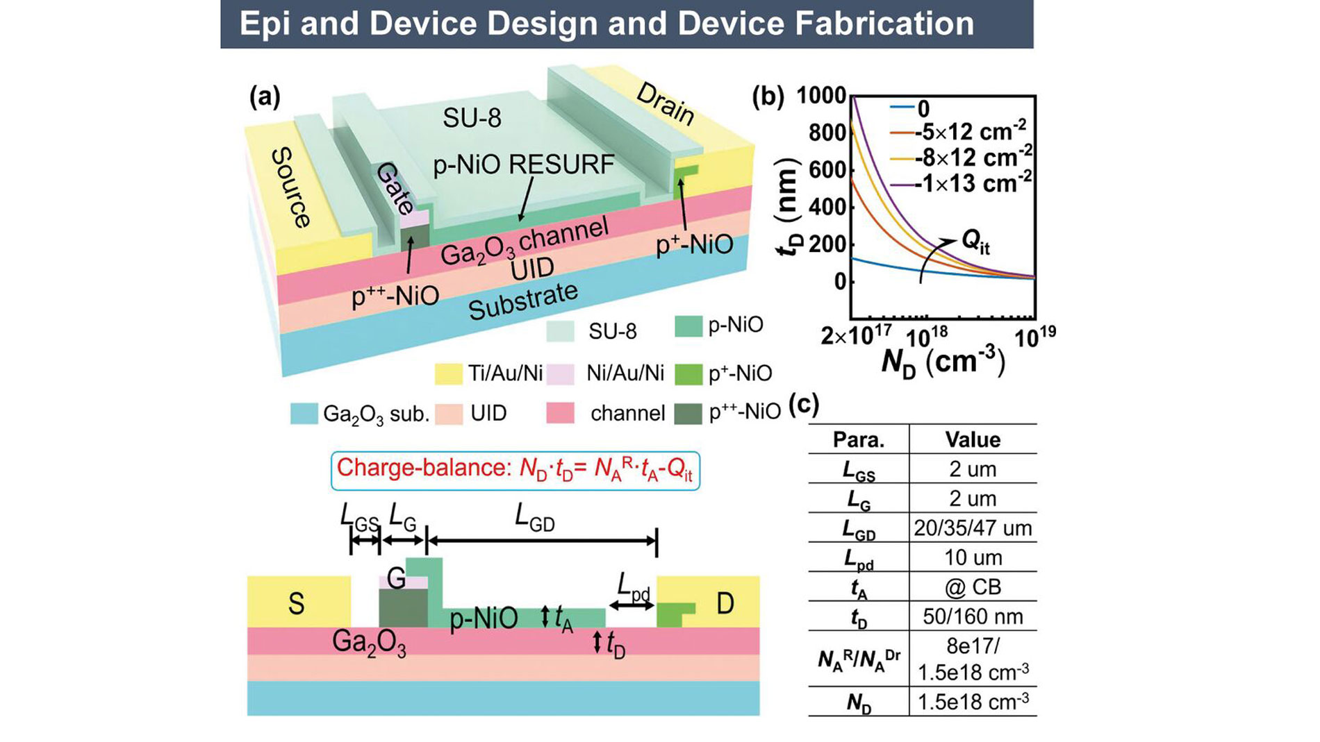
(a) 3-D schematic of the Ga₂O₃ JFET with the p-NiO RESURF and hybrid drain designs. The SU-8 passivation layer is partially removed to show the internal structure. Cross-section view is shown below to illustrate the key geometric parameters and charge-balance (CB) condition. (b) The max channel thickness (tD) as a function of ND to achieve the E-mode, for Qit density from 0 to -1013 cm-2. (c) The list of key device parameters and values. (Source: IEDM 2024)
Design and Fabrication
The Ga₂O₃ JFET is designed with an n-Ga₂O₃ channel (donor concentration ND and thickness tD), a p++-NiO gate, a p-NiO RESURF structure (thickness tA and NA=NRA), and a p+-NiO hybrid drain (NA=NDrA). A spacing between NiO regions prevents punch-through and enables independent doping profiles. Key design aspects are:
E-mode operation: The channel thickness tD and donor concentration ND must satisfy a positive threshold voltage, with ranges shown in simulations.
Charge balance: Matching charge between the p-NiO RESURF and the n-Ga₂O₃-channel yields a superjunction effect, producing a uniform electric field. TCAD simulations confirm that RESURF flattens the E-field, improving breakdown voltage (BV). A hybrid drain suppresses peak fields near the drain, with optimal NA ~1.5×1018 cm-³. Excessive ND, however, crowds the field at NiO spacing, limiting BV.
RON-reduction: Lower RON requires maximizing ND x tD. ND higher than NA of RESURF is preferable to reduce depletion in Ga-Ga₂O₃. Prior studies show NiO doping is tunable (8×10¹⁷–1019 cm-³), so NA of RESURF is set to 8×1017 cm-³. The design space is explored for the best figure of merit (BV²/RON,SP), yielding an optimal ND ~1.5×1018 cm-³. Two channel thicknesses, 50 nm (conservative) and 160 nm (aggressive, considering negative interface charge), are selected.
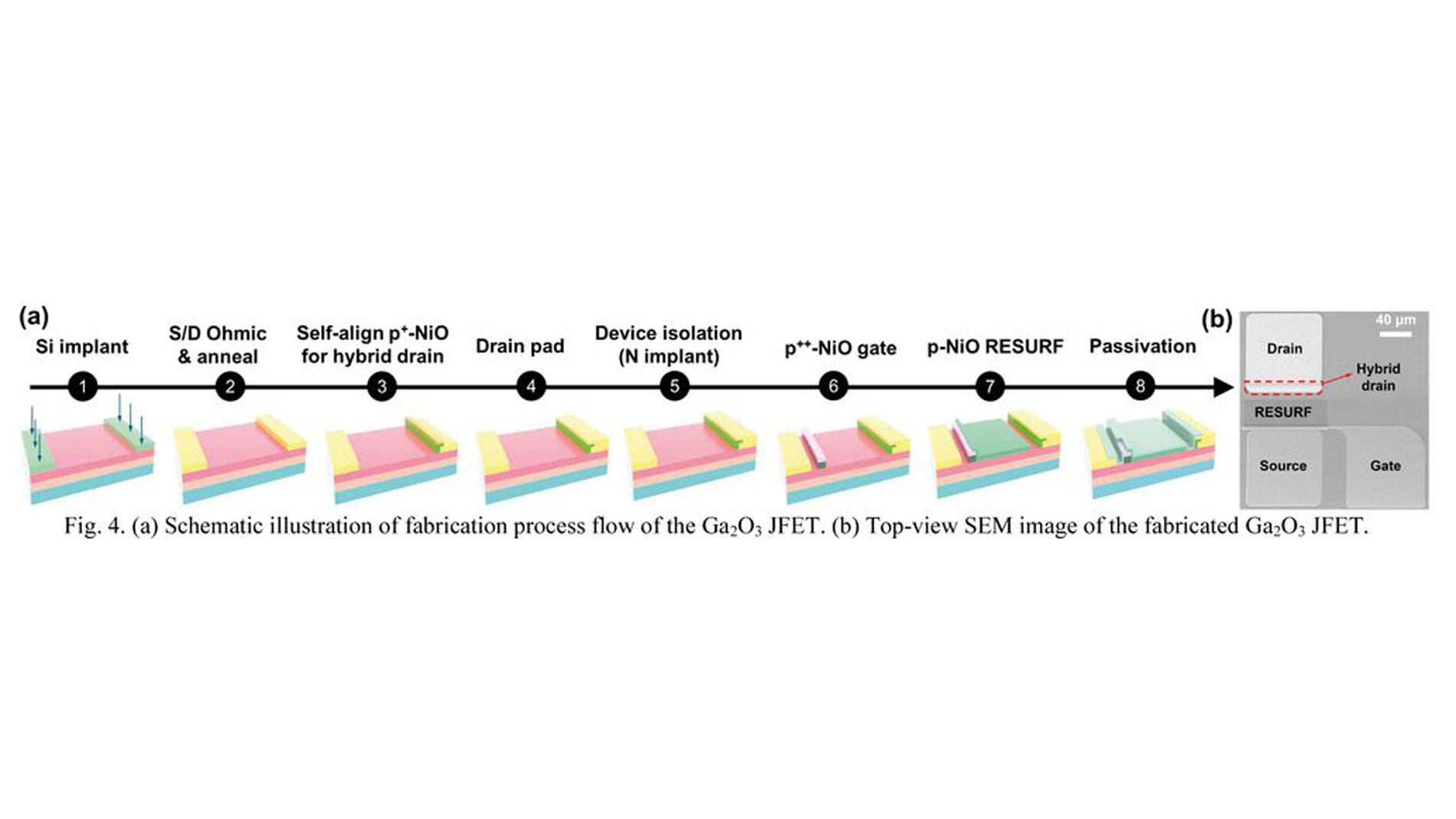
Two Ga₂O₃ devices were grown by MBE on semi-insulating Ga₂O₃-substrates, with measured ND and tD matching targets. Fabrication involved Si implantation, activation, Ohmic contacts, and N implantation for isolation. NiO acceptor concentration was tuned via O2 partial pressure during sputtering to form the hybrid drain, gate, and RESURF. Devices are denoted #A (tD=50 nm) and #B (tD=160 nm), each with variable RESURF thickness and gate-drain spacing (LGD).
Device Characteristics
The electrical performance of Ga₂O₃ JFETs #A and #B was evaluated. At 25 °C, both devices operate in E-mode with threshold voltages of 1.9 V (#A) and 1.5 V (#B), the latter indicating negative interface charge. Specific on-resistances (RON,SP) are 703 and 92 mΩ·cm², respectively, with the much higher RON of #A attributed to a narrower undepleted channel under the gate. The gate voltage range is limited to ~3.5–4 V by leakage, comparable to Infineon’s GaN GITs (Gate Injection Transistors), suggesting compatibility with RC-interface drivers. At 250 °C, #A remains in E-mode (VTH = 0.7 V) with RON only 1.6× higher than at 25 °C, showing lower conduction loss than 10 kV SiC MOSFETs. In contrast, #B loses stability, with VTH turning negative at 100 °C and reaching –3.3 V at 150 °C, rendering gate control ineffective above 175 °C. Breakdown voltage (BV) characteristics show dependence on NiO thickness tA: BV increases with tA, peaks >10 kV at charge balance, then decreases at higher tA. Both devices achieve >10 kV near balance. BV scales with gate–drain distance (LGD), reaching 4346/3516 V, 8560/7275 V, and >10 kV in #A/#B at LGD of 20, 35, and 47 µm, with average lateral fields of 1.75–2.45 MV/cm. At high temperature, BV of #A remains >10 kV up to 250 °C at VGS = 0 V, while #B maintains >10 kV only to 150 °C and requires –10 V gate bias.
Device Reliability and Physics
The researchers at the Center for Power Electronics Systems, Virginia Tech, conducted tests to evaluate the reliability of their Ga₂O₃ JFETs at 150 °C. A Stress–Measurement–Stress method with VGS = 4 V and VDS = 3 kV was applied, while output and transfer characteristics were periodically swept as stress time increased from 1 s to 1000 s. Both devices #A and #B survived the overvoltage HTGB (High Temperature Gate Bias) test, showing threshold voltage and RON shifts within 0.32 V and 35%, which were fully recoverable. Under 3-kV HTRB (High Temperature Reverse Bias) stress, device #A showed shifts of only 0.2 V and 34%, also fully reversible, whereas device #B exhibited a larger negative VTH shift of nearly –3 V, mostly recoverable. The negative shift and BV degradation of device #B at high temperature are attributed to the DIBL (Drain Induced Barrier Lowering) effect: its thicker channel produces a lower barrier and punch-through at high drain voltage (VD), aggravated by interface charge and accelerated de-trapping at elevated temperature. These findings demonstrate that strong gate electrostatic control is critical for reliable high-voltage operation at elevated temperature, even if it requires a trade-off in specific on-resistance as seen in device #A.
(a) Schematic illustration of fabrication process flow of the Ga₂O₃ JFET. (b) Top-view SEM image of the fabricated Ga₂O₃ JFET. (Source: IEDM 2024)
Benchmark and Summary
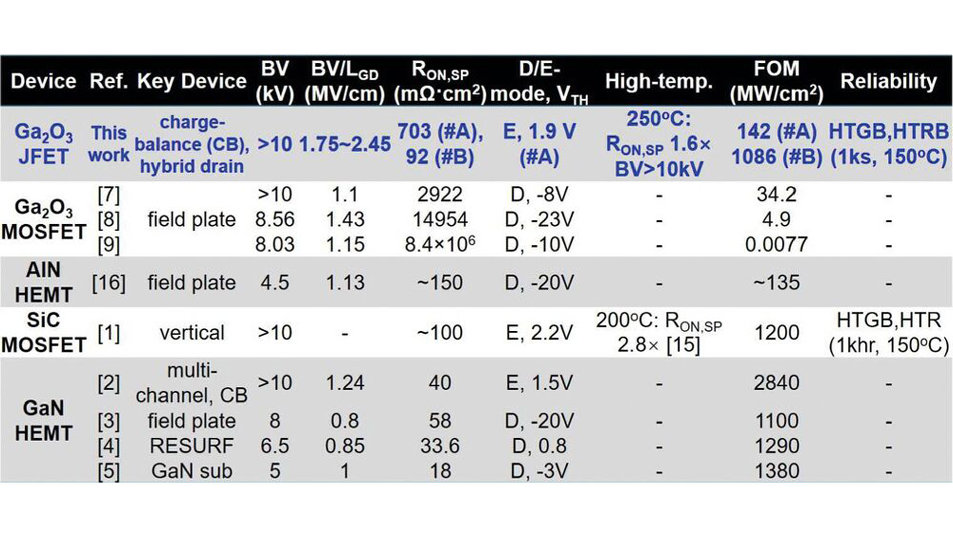
The researchers benchmarked the specific on-resistance (RON,SP) against breakdown voltage (BV) of their Ga₂O₃ JFETs compared with other UWBG transistors above 2 kV. They explained: »The figure of merit (FOM) of devices #A and #B with BV > 10 kV is at least 142 and 1086 MW/cm², respectively, setting a new record among all UWBG transistors with BV > 3 kV.« They further noted that »Device #A is also the first E-mode device reported in this class, while device #B demonstrates an unprecedented balance of low resistance and high voltage.«
Referring to published results in SiC, GaN, Ga₂O₃ and AlN, the team emphasized: »Our device exhibits the highest average electric field and, importantly, provides the first demonstration of 250 °C operation and 3-kV reliability data in a high-voltage transistor beyond SiC.«
In conclusion, the researchers stated: »We demonstrate a 10-kV E-mode Ga₂O₃ JFET with NiO RESURF and a hybrid drain, capable of operation up to 250 °C. Beyond performance advances, the comparison between devices #A and #B highlights the critical role of DIBL suppression at high temperature and kilovolt blocking, offering guidance for the development of future HV, high-temperature power transistors.« (st)
Comparison of the state-of-the-art WBG and UWBG power transistors with BV > 5 kV. (Source: IEDM 2024)