By Ryan Manack, Vice President of Marketing at iDEAL Semiconductor
The global power semiconductor industry faces an unprecedented convergence of supply chain vulnerabilities that threaten the stability of critical electronics manufacturing. Infrastructure costs, geopolitical events, climate change, natural resource shortages and factory shutdowns continue to contribute to ongoing challenges in semiconductor supply chains. To compound this, the demand for power electronics has surged due to a boom in (primarily) the AI, automotive, and renewable energy sectors.
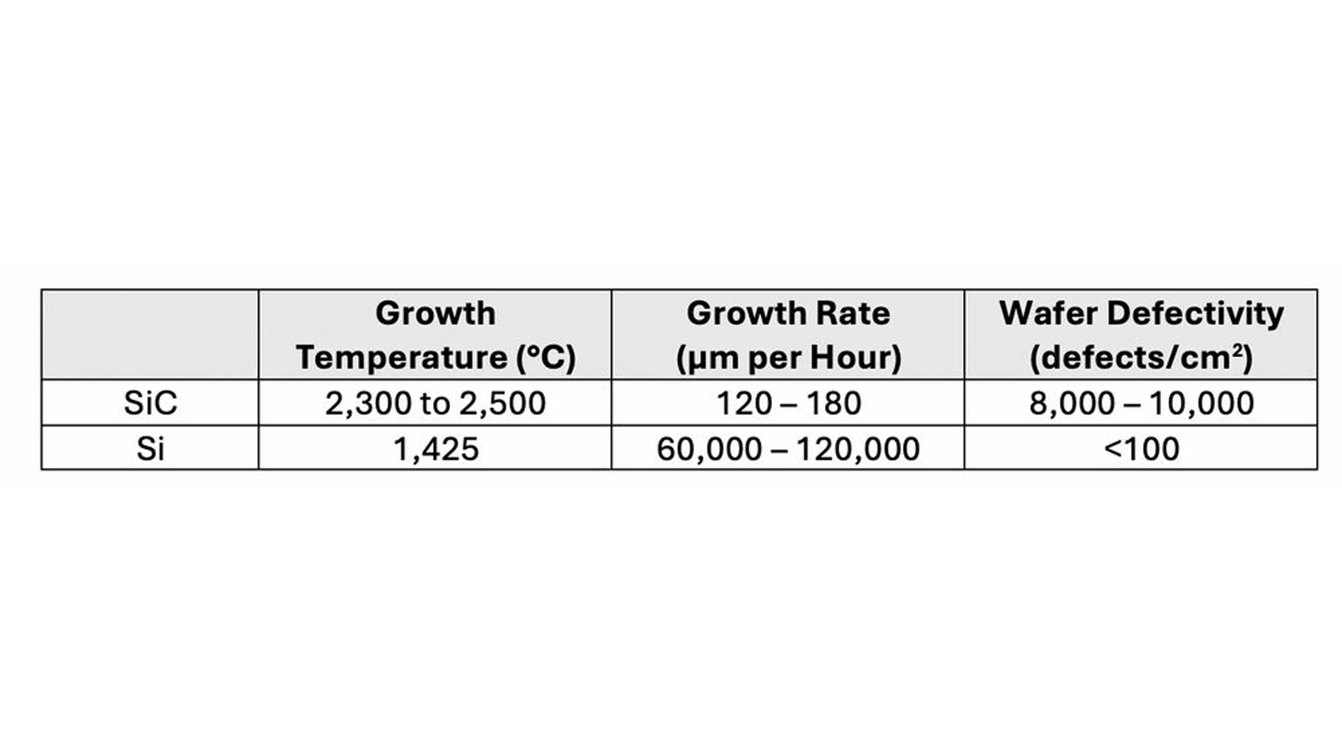
The vulnerabilities in the chipmaking supply chain have particularly affected the growing demand for advanced materials like silicon carbide (SiC) and gallium nitride (GaN). While these wide-bandgap semiconductors offer electrical performance benefits and higher switching frequencies, they face significant procurement challenges due to high costs, primarily from complexities in their growth processes, substrate availability, and defect density issues. For example, SiC boule growth temperature, growth rates, and low wafer yield due to defectivity leads to a far more expensive raw wafer as starting material, prior to epitaxial growth and Power MOSFET wafer processing (see Table 1).
This creates a strategic dilemma for power electronics designers: either accept the performance limitations of traditional silicon or embrace more expensive wide-bandgap alternatives with limited and highly concentrated supply chains: this year alone has seen Wolfspeed enter administration and TSMC stop its production of GaN.
Now, however, a third choice has emerged: a breakthrough in silicon power semiconductor architecture that delivers enhanced performance. SuperQ™ technology developed by iDEAL Semiconductor represents a fundamental shift in power MOSFET design that significantly extends silicon’s performance envelope such as notable reductions in on-resistance (RDSon) and switching losses, without losing any of the conventional advantages of silicon such as proven reliability, low-cost production, and high-volume manufacturing capacity.
Silicon architectural innovation
The evolution of power semiconductor architectures reveals a persistent trade-off designers have had to face between performance and manufacturability. Traditional power MOSFETs, beginning with the 1979 HEXFET design, utilized the entire silicon area for current conduction but suffered from quadratic resistance scaling at higher voltages. Then in 1998, the introduction of reduced surface field (RESURF) architectures, more commonly referred to as Superjunction technology, addressed voltage scaling through 2-dimensional charge balancing, enabling linear resistance scaling with breakdown voltage. However, these architectures sacrifice approximately 50 percent of the die area to non-conducting P-regions, which are dedicated solely to voltage blocking.
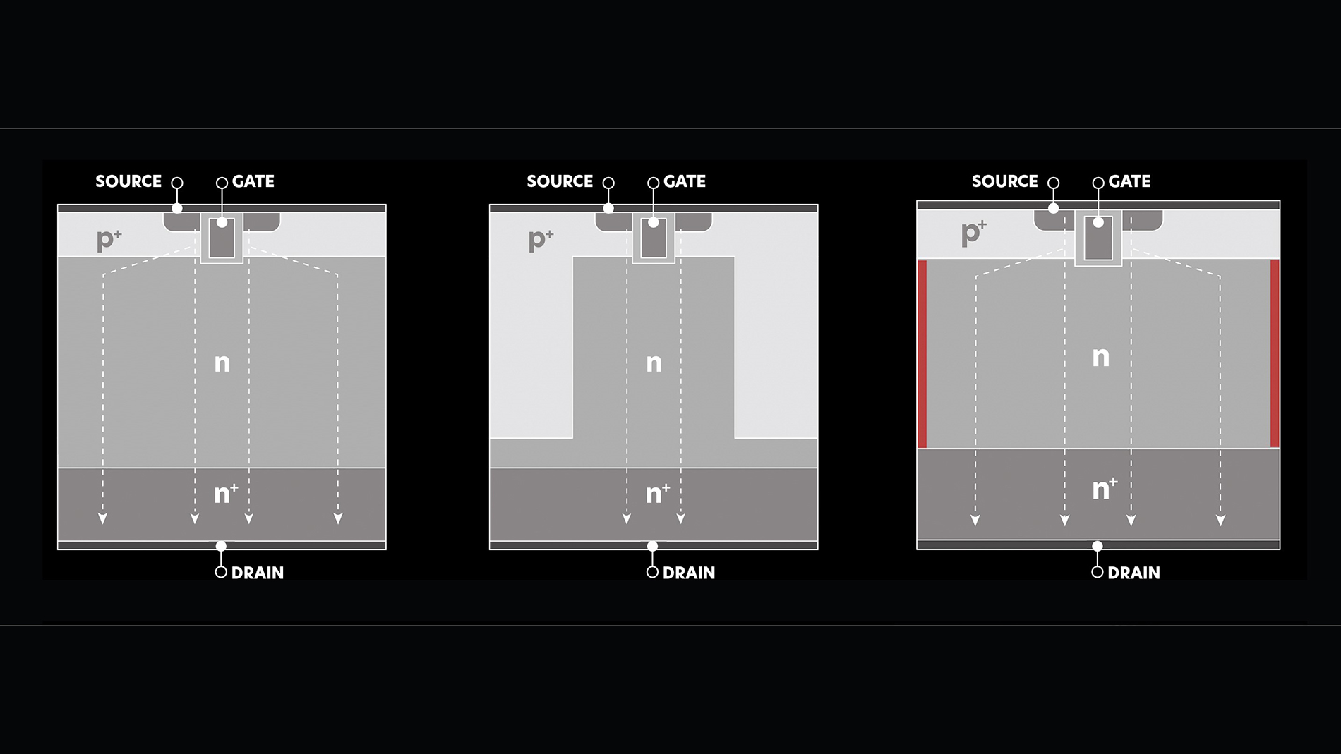
The SuperQ design fundamentally reimagines this approach through an asymmetrical RESURF architecture that maximizes the conduction region (Figure 1). Rather than relying on conventional P-pillars for charge balancing, the technology uses a proprietary high-aspect-ratio deep trench structure with sidewall charge distribution. This architectural shift enables up to 95 percent of the device area to contribute to current conduction, compared to 50 percent or less in traditional Superjunction devices.
SuperQ technology achieves voltage blocking efficiency of 19-20 V/μm while enabling thinner epitaxial layers with optimized doping profiles. This combination results in dramatic reductions in specific on-resistance (RSP), achieving performance that is 2.6× superior to conventional silicon at 200 V, while maintaining full compatibility with standard CMOS manufacturing processes on 200 mm and 300 mm wafers (Figure 2).
Unlike the complex epitaxial growth and implantation processes required for Superjunction devices, SuperQ leverages a streamlined manufacturing flow that prioritizes both performance and cost-effectiveness. The platform’s scalability extends across multiple device types including diodes, MOSFETs, IGBTs, and power ICs, covering voltage ranges from 60 V to 1,200 V.
Quantified performance advantages
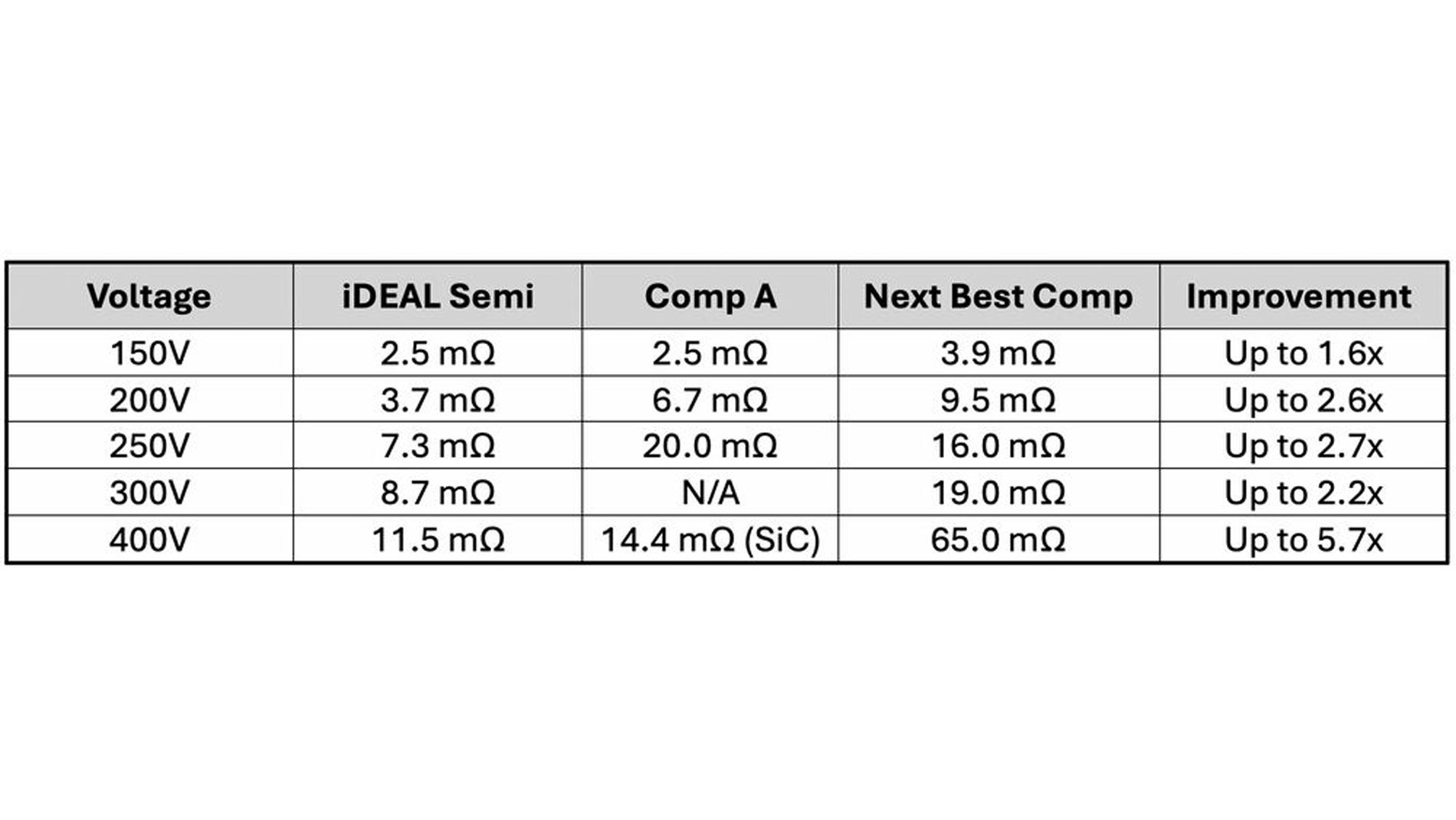
SuperQ devices demonstrate measurable improvements across silicon MOSFET figures of merit (FOM) that directly impact system efficiency and thermal management. In conduction performance, the 150 V technology achieves on-resistance as low as 2.5 mΩ in TOLL packaging, matching industry-leading devices while providing 1.6× improvement over nearest competitors. At 200 V, SuperQ devices achieve 3.7 mΩ in TOLL packaging, representing nearly 50 percent reduction compared to the current industry leader and a 2.6× improvement over the next-best competitor.
The performance advantage extends to higher voltages where traditional silicon typically cedes ground to wide-bandgap alternatives. At 400 V, SuperQ capabilities in TOLL packaging not only exceed conventional silicon but also outperform the industry’s best SiC devices at equivalent voltage ratings.
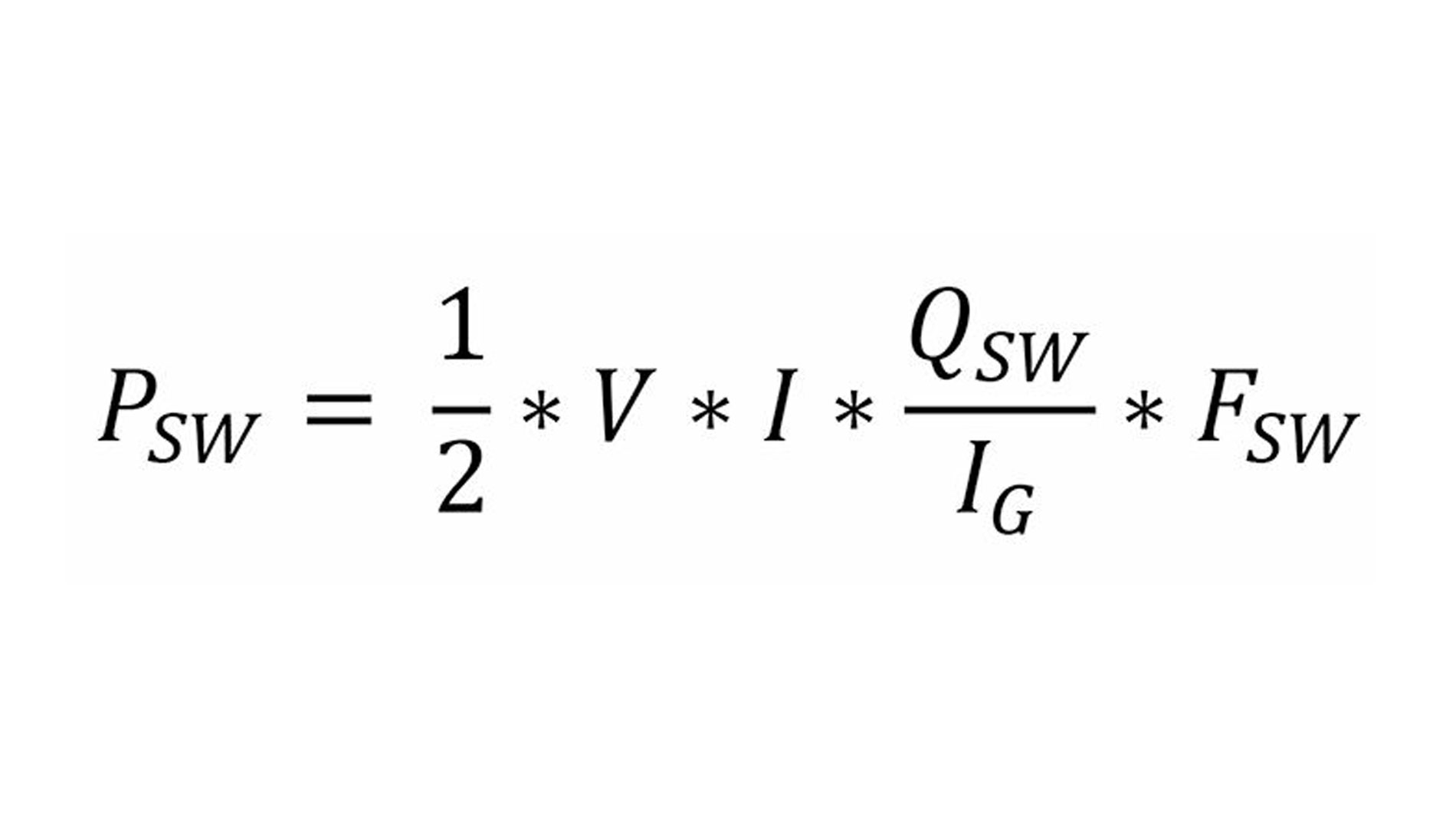
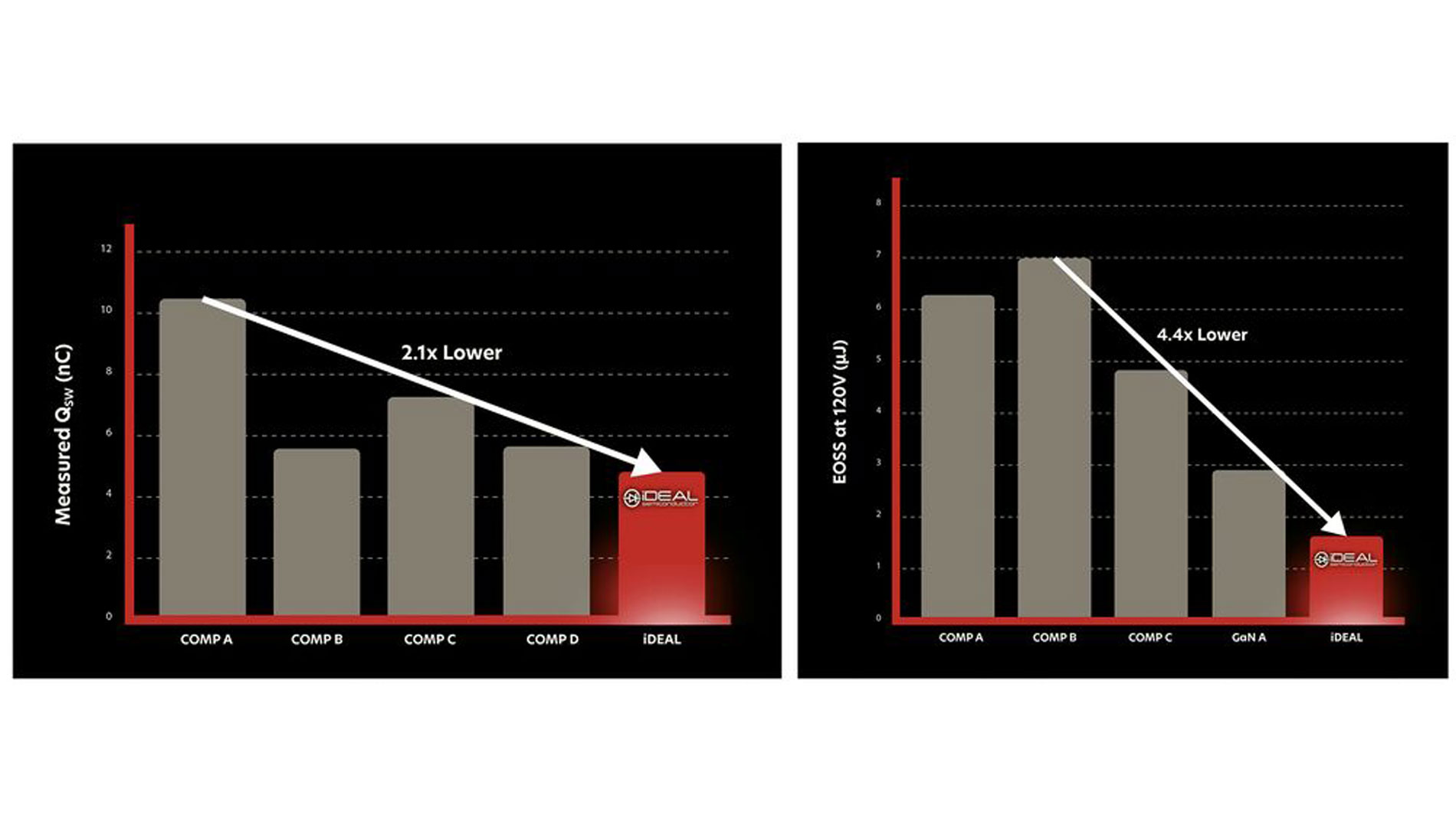
Switching performance metrics reveal equally significant advantages. Switching charge (QSW) reduction reaches up to 2.1× compared to leading silicon competitors (Figure 3), directly translating to faster switching times and reduced switching losses according to the following relationship:
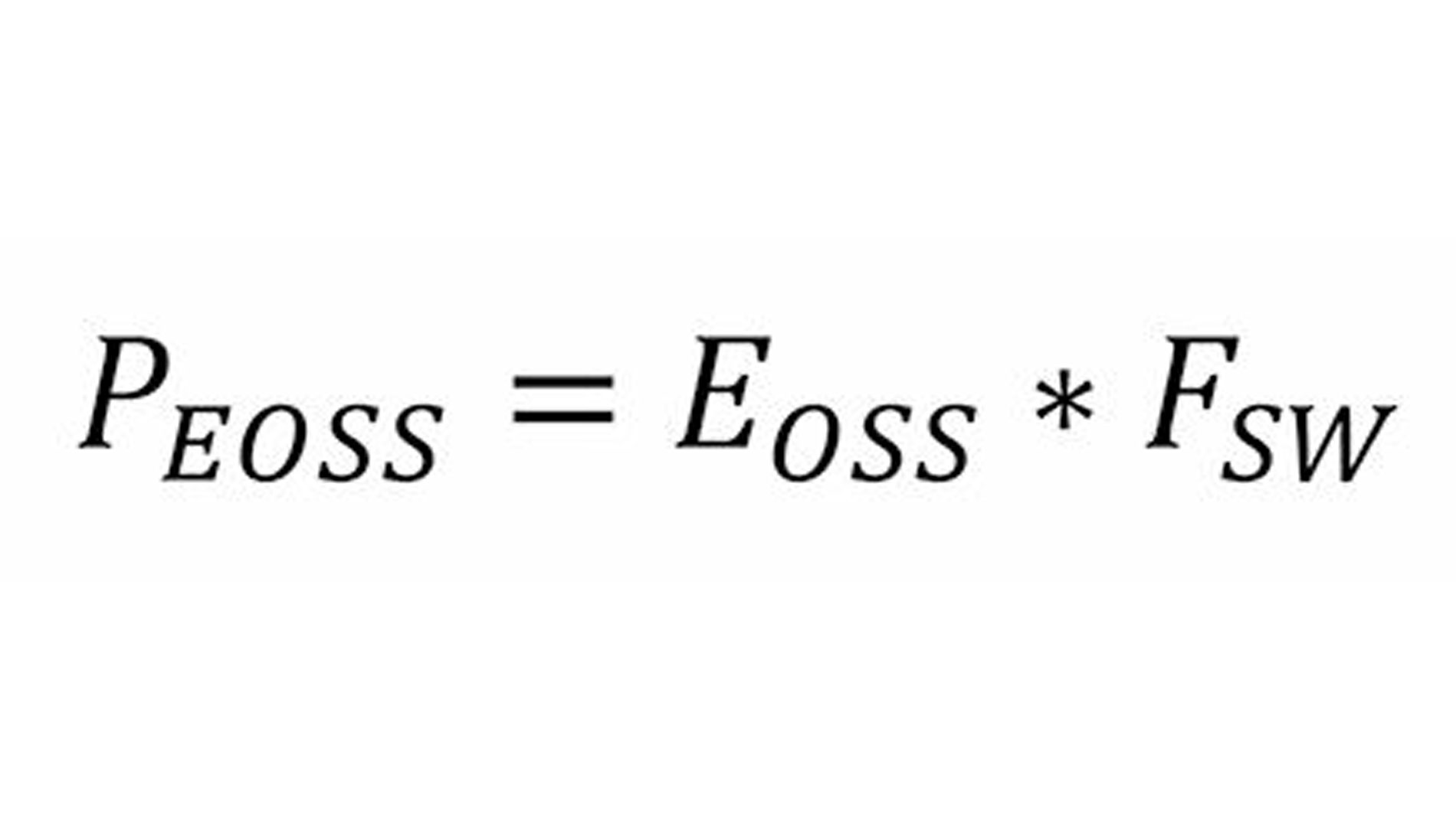
This improvement enables higher switching frequencies in demanding topologies or proportional power loss reductions at equivalent frequencies. Additionally, SuperQ devices store significantly less energy in output capacitance (COSS), achieving up to 4.4× reduction compared to silicon alternatives. Remarkably, even compared to industry-leading GaN devices, capacitive stored energy (EOSS) is reduced by 50 percent, minimizing capacitive switching losses governed by:
These combined improvements in conduction and switching performance enable system designers to achieve higher power density and efficiency while operating within familiar silicon design paradigms.
Manufacturing resilience and supply chain advantages
The strategic importance of SuperQ technology extends beyond pure performance metrics to encompass supply chain resilience in an increasingly uncertain geopolitical environment. The technology’s compatibility with standard silicon manufacturing processes ensures access to the industry’s most mature and geographically distributed production capacity.
Standard 200 mm and 300 mm silicon fabrication facilities worldwide can manufacture SuperQ devices without requiring specialized equipment or rare materials. This contrasts sharply with SiC and GaN production, which depends on limited substrate suppliers, specialized epitaxial growth equipment, and tightly controlled manufacturing processes that restrict production to a small number of facilities.
The CMOS-compatible manufacturing flow ensures high yields and enables rapid capacity scaling through existing foundry partnerships. This approach significantly reduces supply chain risk while maintaining cost competitiveness; critical factors as the industry navigates ongoing materials restrictions and manufacturing capacity constraints.
Production scalability is demonstrated through iDEAL Semiconductor’s commercial rollout, with 150 V and 200 V SuperQ MOSFETs entering full production in July 2025. Higher voltage variants spanning 250 V to 400 V are progressing through development pipelines, leveraging the same fundamental manufacturing processes to ensure consistent supply availability.
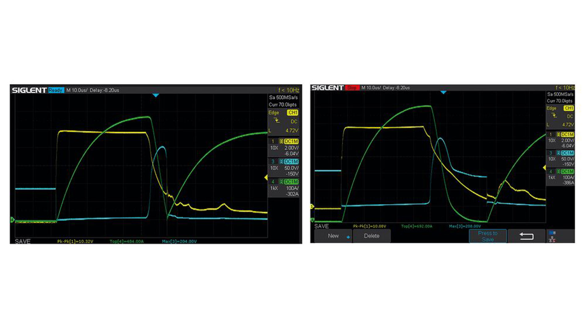
Peak short-circuit current to failure for Competitor A (left, 570A) and SuperQ (right, 692A) for similar RDSon and silicon area. Green = Drain Current, Blue = Drain-to-Source Voltage, Yellow = Gate-to-Source Voltage
Application-driven performance validation
Real-world application testing validates SuperQ technology’s practical benefits across diverse power conversion scenarios. In AI data center applications, where 54 V server architectures demand both efficiency and reliability, SuperQ MOSFETs serve as synchronous rectifiers with demonstrable thermal advantages.
Telecommunications infrastructure applications have shown similar benefits, where SuperQ devices function as primary-side control MOSFETs in isolated DC/DC converters. A commercially deployed 270 kHz Active Clamp Forward topology demonstrates SuperQ’s impact on system reliability and operational lifetime. In a 48 V input, 12 V output, 17 A configuration, SuperQ devices reduce power losses by up to 2 Watts compared to leading competitors while operating 31 °C cooler under identical conditions.
In brushless direct current (BLDC) motor drives, the versatile and robust SuperQ can be used for both three-phase inverter switching as well as battery protection. When deployed in battery disconnect switching applications, the devices combine industry-leading on-resistance with exceptional short-circuit current handling, withstanding fault currents up to 700 A, significantly exceeding comparable silicon devices with similar resistance and die area (Figure 4).
SuperQ technology has undergone comprehensive JEDEC qualification testing including HTRB, HTGB, thermal cycling, BHAST, IOL, HTSL, and UHAST protocols, with stress levels exceeding standard requirements by at least 2×. The devices maintain stable operation to 175 °C junction temperatures with wide safe operating area (SOA) margins, ensuring robust performance in demanding industrial, automotive, and data center environments.
Strategic design implications
SuperQ technology addresses a fundamental challenge facing power electronics engineers: achieving advanced performance without compromising supply chain security or cost competitiveness. As geopolitical tensions continue to affect semiconductor availability and wide-bandgap materials face ongoing cost and supply constraints, silicon-based innovations that extend performance may become a strategically wise choice.
The immediate commercial availability of SuperQ technology provides design teams with a more practical path to quantifiable performance improvements without the supply chain concentration risks inherent in wide-bandgap alternatives, while still delivering cost structures compatible with high-volume production requirements. As power conversion requirements will continue to expand in the future across vehicle electrification, renewable energy, and digital infrastructure sectors, SuperQ technology is an excellent example of how strategic innovation within established manufacturing ecosystems can address both performance demands and supply chain vulnerabilities. eg