Stefaan Decoutere, imec fellow and program director, gallium nitride (GaN) and power electronics
One of the driving forces behind GaN technology development is the need for decarbonization and energy efficiency across industries. Mass production is currently ramping up, with multiple semiconductor companies breaking through. But success also hinges on the ability to establish a robust ecosystem and jointly drive innovation from GaN growth to packaging solutions. Just as in CMOS, developing GaN power electronics requires close coupling between design, epitaxy, process integration, and applications.
Today, the bulk of GaN R&D efforts focus on three types of devices: lateral high-electron mobility transistors (HEMTs), bi-directional switches, and vertical GaN field-effect transistors (FETs).
Lateral HEMTs: industry’s workhorse for power converters
Virtually every GaN power transistor on the market today is composed of a lateral AlGaN/GaN-based HEMT structure. In this lateral configuration, the three transistor terminals (source, gate, and drain) reside at the surface, in the same plane. By a gift of nature, the two-dimensional electron channel at the AlGaN/GaN interface forms spontaneously, with no need for external gate bias. This means the device is normally on and requires a negative gate bias to deplete the channel and turn it off: it is a depletion mode or d-mode device. D-mode devices are the preferred choice for applications operating at high power and voltage levels. Think about on-board chargers for automotive, for which the low on-resistance of the conduction channel is a critical metric.
Most of the embedded power electronics systems, however, require normally-off (enhancement mode or e-mode) devices for fail-safe operations. The HEMT device architecture, therefore, must be modified to allow e-mode operation. The most widely used approach is to add a p-type doped GaN layer under the gate electrode.
Imec works only on e-mode p-GaN gate power devices. Focus is on e-mode p-GaN HEMTs GaN-on-Si substrates. These lateral p-GaN gate e-mode devices form the basis of a mature p-GaN HEMT platform for a variety of power electronics applications. By engineering the material stack and using adequate substrates, different p-GaN HEMT devices with operation voltages ranging between 40 and 650V have been demonstrated. In case thick buffers are required such as for 1200V and higher on 200mm substrates, or for 650 V and higher for 300mm, we work on engineered substrates (QST substrates). Imec experimentally demonstrates a 1.2 kV normally-off p-GaN gate lateral high-electronmobility transistors (HEMTs) on 200 mm diameter engineered substrates. The fabricated p-GaN HEMTs exhibit an on/off ratio of 108, a low specific on-resistance of 5.8mΩ/cm2, and a hard breakdown voltage as high as 1,800V. These features make the 1,200V p-GaN HEMTs attractive building blocks for in-rack power distribution systems in data centers, which tend to move to 800V and beyond.
Progress on e-mode devices has been substantial such that most applications today are done or can be done with this type of devices. E-mode power devices can alternatively be made in so-called cascode d-mode HEMT configurations, where a d-mode HEMT is combined with a Si-based lower-voltage power device. While the HEMT enables operation at high voltages, the Si-based power device ensures fail-safe operation.
Bi-directional switches: potential for battery protection and AC/AC converters
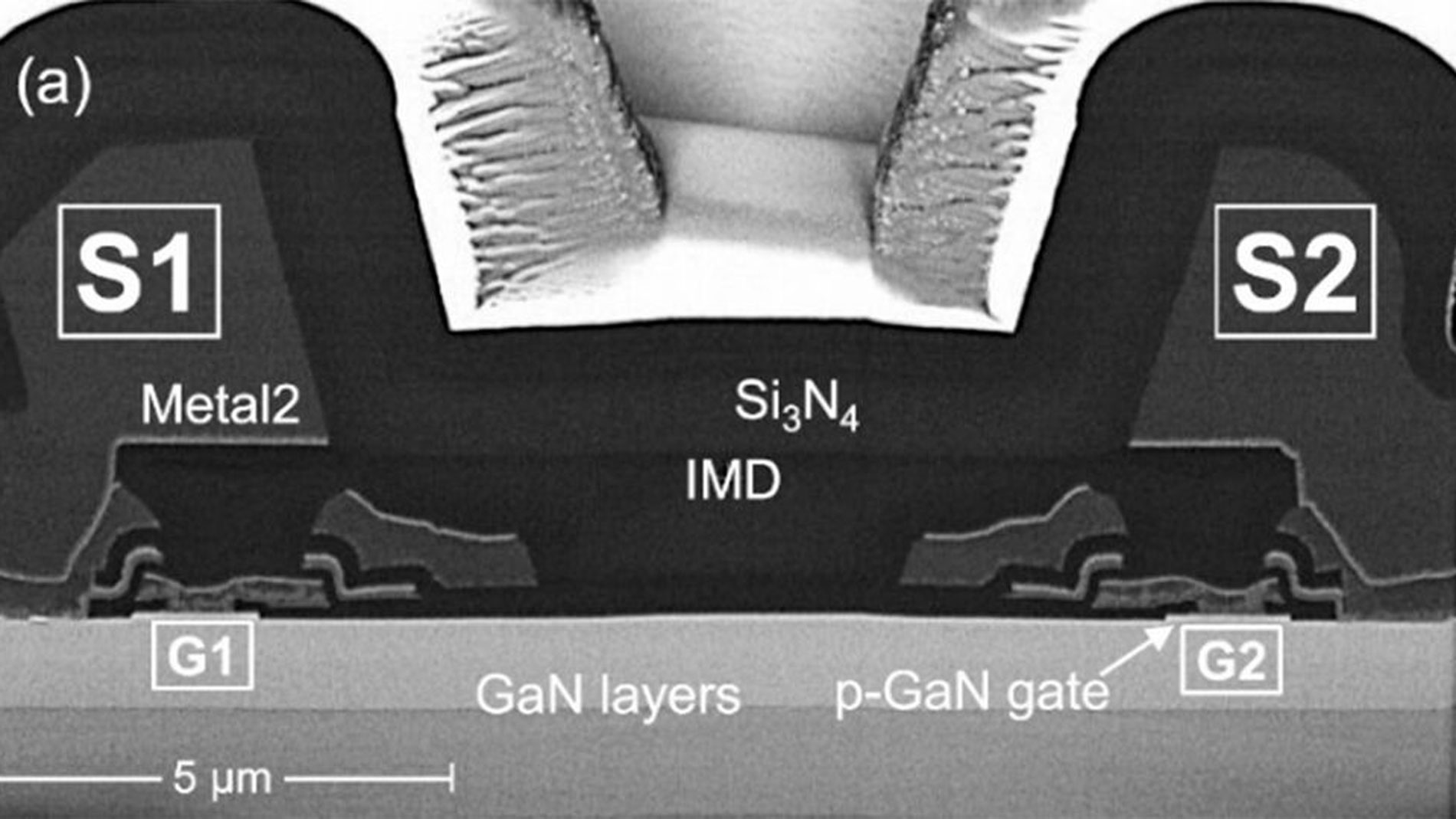
Lateral p-GaN HEMTs are traditionally used to serve AC/DC or DC/DC converter operations. Their device architecture can be modified to enable bi-directional switches, which conduct current and block voltage in both polarities. Such switches are desired, for example, in battery protection circuits and matrix converters – efficient AC/AC converters that do not require a DC link. In traditional Si implementations, a bi-directional switch is formed by connecting two discrete unidirectional MOSFETs or IGBTs in anti-parallel or anti-series configuration. GaN HEMT technology offers a much simpler design approach by adding a second gate to a conventional HEMT structure. By using this dual-gate architecture, imec demonstrated 650V and 1200V p-GaN bi-directional switches, providing symmetrical electrical operation in positive and negative bias conditions while achieving comparable performance to traditional HEMTs. We explored diode bridge, anti-series and anti-parallel topologies as well, but could not find a performance advantage compared to the dual-gate and single reference switches. Currently imec is working on second generation bi-directional switches with engineered gates, optimized field plates and (in case of dual-gate bi-directional switches) on a substrate bias management circuit. GaN Bi-directional switches are already in production, e.g. for battery protection and management in latest cell phones (low voltage) and e-bikes (medium voltage). Main application at higher voltage targeted is for OBCs.
Vertical GaN devices: an alternative for beyond 650V operation
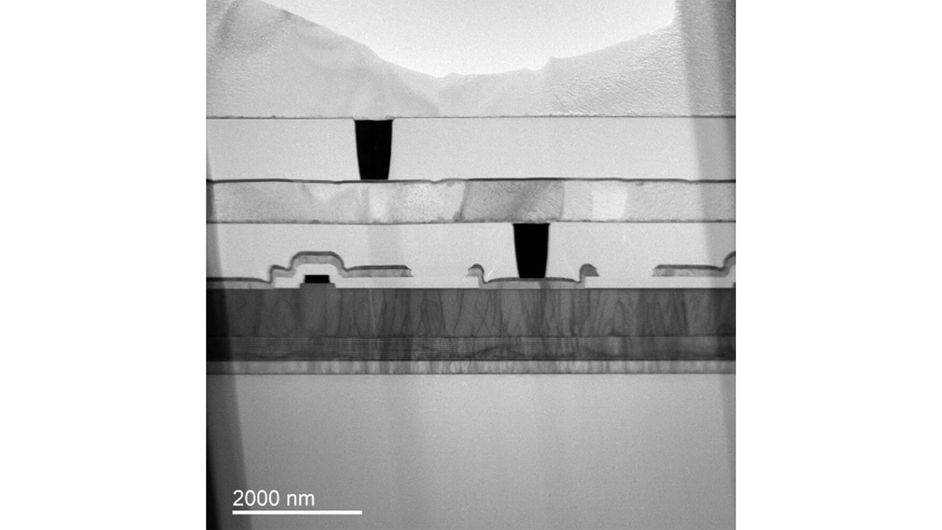
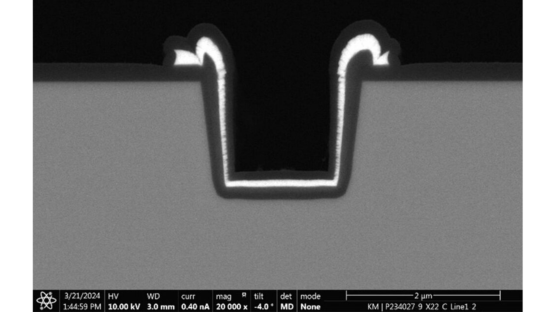
Lateral GaN HEMTs are used for high frequency applications, in contrast, vertical GaN FETs are suitable for high power. This is because lateral p-GaN HEMTs for voltages higher than 650V have two disadvantages in terms of footprint: the gate-to-drain distance needs to increase for higher breakdown voltage and robustness, which in turn increases the on-state resistance. Hence, the footprint of the HEMT increases quadratically with the voltage for the same specific on-state resistance. A vertical GaN-based MOSFET device is being explored as an alternative device architecture for beyond 650V operation. In a vertical GaN device, the source and gate are at the device surface, but the drain is fabricated at the bottom of the epi stack. As such, the electrical field is spread vertically throughout the whole material stack. Main difficulties for 1200 Volt vertical GaN FETS is the termination of the device, and reliable ohmic p-body contact using CMOS-compatible materials (e.g. no Au). Imec has submitted several patents on new vertical device architectures with higher current densities. Different vertical architectures are being investigated, including a trench-gate MOSFET architecture as shown by imec. In 2024 imec proposed a path to commercially viable vertical GaN devices using 200-mm QST (Qromis substrate technology) engineered substrates, scalable to 300 mm and CMOS-compatible. QST wafers use a poly-AlN core with thermal expansion matched to GaN, enabling growth of thick GaN layers without wafer breakage. This overcomes the fragility issues of GaN-on-Si at large diameters and supports manufacturable vertical GaN technology.
Further on the horizon: multi-channel devices and more
Among the notable developments of the past years are multi-channel GaN devices, offering similar advantages as gate-all-around devices for traditional logic CMOS applications: larger current density at a reduced footprint, while preserving a low off current and series resistance. GaN is a relatively young technology with much room for further device exploration. In the years to come, we expect many innovations serving next-generation power electronics devices.
The lack of p-channel GaN HEMTs: industry’s workarounds
One major concern has long occupied GaN researchers: there are no p-channel GaN devices that can operate at an acceptable level of performance. CMOS designs use a combination of n- and p-channel devices to ensure the most efficient performance of logic operations. But in GaN, the mobility of holes is about 60 times worse than that of electrons. That means a p-channel device – where holes are the principal carriers – would be 60 times larger than the n-channel counterpart. This ‘asymmetric’ configuration of n and p would be highly inefficient. Industry gets around this issue in several ways. In resistor-transistor logic, the p-channel device is replaced with a resistor. Although this comes with a trade-off between switching time and power consumption, it works well enough for many power electronics circuits like inverting functions in logic gates and analog circuits. To overcome some of the disadvantages of using a resistive load, a current source can replace the resistor. This current source can be a p-GaN island d-mode device or a MISHEMT d-mode device (with Vgs = 0 Volt hardwired). An alternative is direct-coupled FET logic (DCFL), resulting from the co-integration of d-mode and e-mode HEMTs. Both solutions are pursued by imec. A more disruptive approach uses n-channel GaN HEMTs with Si pMOS devices, using 3D integration techniques to stack the two devices.
Substrates for GaN epitaxial growth: upscaling to 200 and 300mm wafer sizes
The performance of GaN devices is not only determined by the material stack and device architecture but is also strongly linked to the substrate on which the GaN material stack is grown. What is more, the choice of the substrate is of paramount importance in determining whether GaN technology is economically viable.
From a technical point of view, native GaN substrates offer the best material quality. But they are expensive and, so far, only available on small wafer diameters (up to 150mm (6-inch)). As such, they can hardly follow the trend that marks the power electronics industry today: 200mm (8-inch) substrates have become an industry standard, and upscaling to 300mm (12-inch) is considered whenever feasible.
In 2025 Imec has launched his 300 mm GaN program, initial partners are AIXTRON, GlobalFoundries, KLA Corporation, Synopsys, and Veeco. This program track, part of imec’s industrial affiliation program (IIAP) on GaN power electronics, has been set up to develop 300mm GaN epi growth, and low and high voltage GaN high electron mobility transistor (HEMT) process flows. There are three reasons why GaN on 300mm wafers is interesting:
- Cost reduction for wafer size scaling,
- access to advanced dielectrics and lithography,
- possibility to bond a 300mm GaN power wafer with other 300mm substrate. Prime concerns are the control over the bow of the 300mm wafers and their mechanical strength. As these issues worsen for thicker material stacks, which are needed for high-voltage applications, the first use cases for 300mm GaN-on-Si will be in the lower voltage range. Examples are PoL converters for CPUs and GPUs. These processors typically operate at low output voltages (around 0.5V) but require extremely high currents, often exceeding 1,000A. Advanced GaN PoL converters promise to efficiently manage this power delivery without excessive losses.
In this program the partners wanted to find solutions to overcome following problems in the initial phase:
- Wafer handling of GaN-on-Si wafers (low voltage) or GaN-on-QST wafers (high voltage),
- contamination control,
- building up experience with the optimization of the GaN/AlGaN stacks in the new 300mm MOCVD reactors.
To make this program successful, the whole supply chain has to be set up for 300mm wafers, for Si 111 wafer availability as starting material, MOCVD growth on volume production tools, wafer processing, wafer grinding, backside metallization, dicing etc. imec expects, that a commercial production based on 300 mm wafers could start 2027/2028.
For higher voltage applications, industry looks at alternatives such as QST (Qromis substrate technology), a material with a polycrystalline AlN core and which is already commercially available. Compared to Si, QST is better matched with the GaN/AlGaN buffers in terms of thermal expansion. The mechanical strength of QST and its capability to more easily control the wafer bow have already been demonstrated on 200mm wafers, and 300mm semi-spec and CMOS-compatible QST engineered substrates are under development. 200mm QST was the substrate of choice for imec’s 1,200V p-GaN HEMT devices and vertical GaN FETs.
Other substrates are being looked at for specific power electronics applications, but today they are mainly in the research phase: gallium oxide (Ga2O3) and SiC-on-Si. A new and promising substrate on the horizon is enabled by Soitec’s Smart CutTM of GaN (SmartGaN technology), where a monocrystalline GaN seed layer is fabricated on top of a poly-crystalline SiC core wafer.
Trends in circuit and system development
Initially, most GaN-based power systems have been formed from multiple chips. The GaN switches are assembled as discrete components and connected to other, non-GaN-based components through a printed circuit board (PCB). The downside of such an approach is the presence of parasitic inductances that affect the performance of the devices. Take a gate driver, for example, a component that supplies current to the GaN transistor’s gate to turn it on and off. Discrete GaN transistors with drivers on a separate chip suffer from parasitic inductances between the output stages of the driver and the input of the transistor. The best way to reduce the parasitics and exploit the superior switching speed of GaN is to make both driver and HEMT in GaN technology and integrate them on the same chip. Such monolithic integration has long proven difficult, mainly due to the lack of complementary GaN-based devices and difficulties in obtaining power domains on a single die for isolating the different components.
But in recent years, tremendous progress has been made in monolithically integrating GaN power switches with other building blocks. Different R&D approaches are being pursued. On the one hand, limited functionality is monolithically co-integrated to make the GaN power device more intelligent and robust. Examples of such ‘smart discretes’ arise from the co-integration with current sensors, temperature sensors, the output stage of a gate driver, and over-voltage protection circuitry. On the other hand, we see power electronics systems emerge with maximal monolithic integration, including half-bridges, full gate drivers, floating supply voltages, isolated level shifters, dead-time control, and protection circuitry, etc.
Imec has demonstrated the monolithic integration of a variety of GaN components using its GaN-on-Si, GaN-on-QST, and GaN-on-SOI (Si-on-insulator) technology platforms. An example is a monolithic 200V GaN half-bridge IC with integrated gate drivers and level shifters.
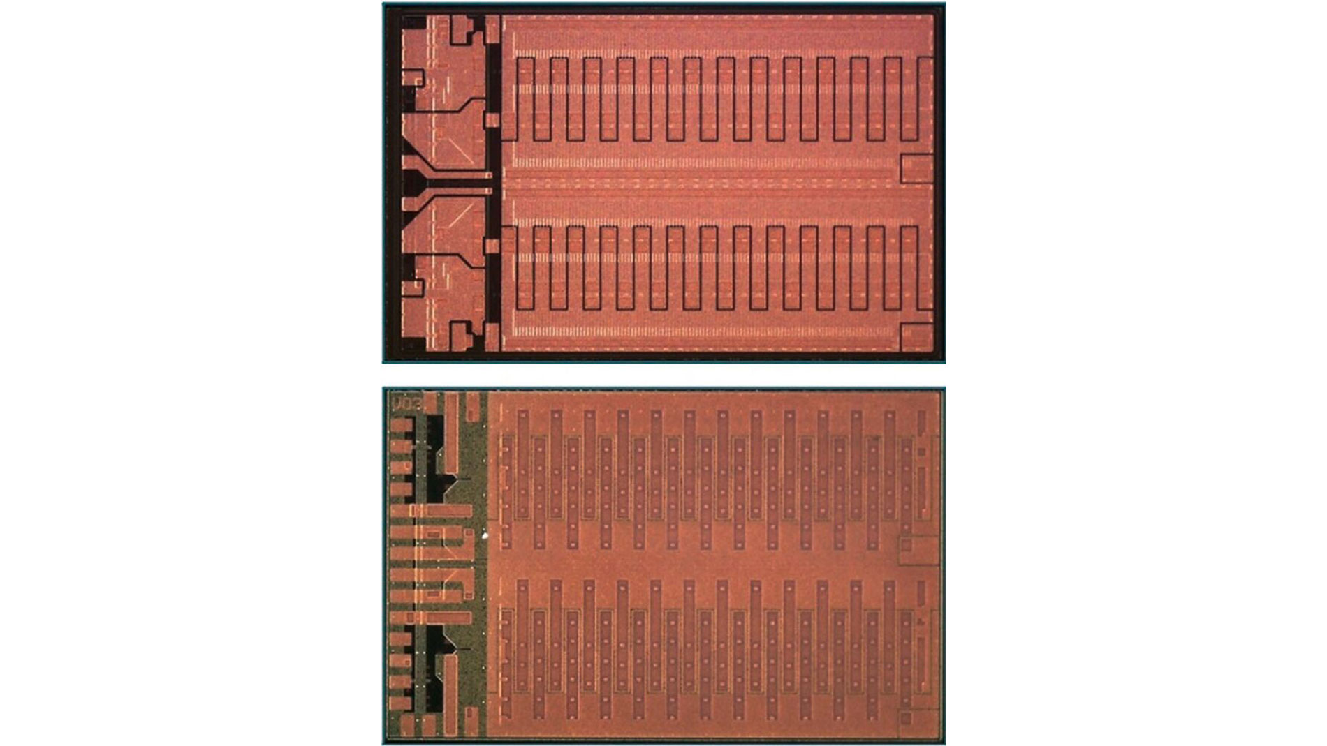
A half-bridge circuit is a fundamental topology used in power electronics, and consists of two semiconductor switches (here, p-GaN HEMTs) connected in series. In DC/DC converters, for example, a half-bridge converter efficiently steps down or steps up DC voltages. A monolithic half-bridge IC design with integrated drivers and level shifters, manufactured on imec’s GaN-IC platform, resulted in highly efficient conversion capabilities over a range of realistic operating conditions, with 98.3 percent peak power stage efficiency. Other examples are imec’s half-bridges, which are monolithically integrated with drivers, current and temperature sensing circuits, both for 100V and for 650V applications. Additionally, high-performance GaN Schottky barrier diodes were added to the portfolio, enabling further enhancement of the power efficiency of GaN power ICs.
The monolithic half-bridge is fabricated using are baseline GaN-IC platform, which when processed on Si substrates is similar to the discrete flow. If the application cannot tolerate back-gating effects, this can be eliminated by processing on SOI or QST wafers with oxide-filled deep trench isolation, or by using a two-die solution with separate high-side and low-side chips, or by using different type of substrate such as sapphire. Monolithic ICs are entering the market, but with large differences between the level of integration and solutions proposed.
Besides an increased level of monolithic integration, we also see examples of hybrid integration emerging for tailored performance. An example is an 800V inverter made from a combination of GaN-based 650V bi-directional switches and 1,200V SiC-based switches. Or Si-based BCD chips (chips that combine Si-based bipolar, CMOS, and DMOS technologies) with a GaN device on top, integrated with die-to-wafer or die-to-die 3D integration techniques.
The power electronics industry is not a ‘winner-takes-it-all’ market. We will see various combinations coexist, trading off power conversion efficiency, design simplicity, speed, robustness, size, and cost to the benefit of the application. With this goal in mind, increasing attention is also being paid to system-level optimization rather than component-level optimization.
Reliability, robustness, and packaging: crucial factors for technology adoption
Reliability, robustness, and packaging are also critical factors for the successful adoption and integration of GaN devices into various applications.
At the device level, reliability is affected by the management of peak electrical fields through field plate designs, charge trapping in the dielectric close to the interface with the AlGaN polarization layer, and the quality and defectivity of the epitaxial layers. Advancements in the metal-organic chemical vapor deposition (MOCVD) growth technique and process control have played a pivotal role in mitigating these challenges. One peculiarity of p-GaN HEMTs is their shorter lifetime at lower temperatures (e.g., -25°C) when operating under forward gate voltage bias. This can be explained by a negative activation energy of the failure mechanism. This can be of importance for certain applications and operating conditions (e.g., deploying GaN-based devices in northern countries) and necessitates extending (gate) reliability tests in the low temperature range.
GaN reliability should, however, not only be considered at the device level. Reliability and robustness can be enhanced at the system level by adding components and circuits that help control the GaN transistors’ gate and suppress transients – i.e., temporary changes in voltage or current that occur during switching operations. Under-voltage lockouts, overcurrent protection, and temperature sensors that feed their data back to the gate drivers are all crucial to unleashing the full performance and reliability of GaN switching devices.
And finally, the high-voltage and high-power capabilities of the GaN-based devices and systems necessitate effective packaging solutions that can handle high voltages and temperatures without causing electrical breakdown. st
Author
Stefaan Decoutere received his M.Sc. degree in Electronic Engineering and his Ph.D. degree from the Katholieke Universiteit (KU) Leuven, Belgium, in 1986 and 1992, respectively. He has been at imec since 1987, where he started in high-voltage BCD technology development. From 1992 to 1997, he was responsible for the development of high-speed BiCMOS and SiGe HBT technologies. In 1998, he became the head of the Mixed Signal/RF technology group in imec. Since 2010, he has managed GaN Power Device technology development, and in 2015, he became the director of the GaN technology program. In 2023, he became an imec Fellow.