By Dr. Oliver Hilt, Head of the Wide-Bandgap Electronics Department at Ferdinand-Braun-Institut (FBH)
Power converters are key components of modern energy systems, enabling efficient energy conversion and management across industries ranging from renewable energy and electric mobility to smart-grid infrastructure. To meet the requirements of these demanding applications, they must deliver even higher efficiency, increased power density, and enhanced thermal management. This also requires incorporating advanced semiconductor materials like silicon carbide (SiC) and gallium nitride (GaN) to boost device performance of diodes and switches. Future designs will prioritize scalability, high-voltage performance, and cost effectiveness to address the growing demands of electrification driven by clean-energy goals and digitalization.
Already commercialized SiC-based power transistors feature a vertical chip design with the low-voltage and high-voltage terminals separated at the top and bottom of the chip. Typical blocking voltages range from 900 V to 1700 V, with transistors designed for power conversion > 2 kW. Today’s GaN-based transistors use a lateral design architecture, with all three terminals located on the top side of the chip. Blocking voltages typically range from 48 V to 800 V and offer an extremely low gate charge, resulting in minimal switching losses. This combination achieves highest efficiencies at even higher power densities. In practice, GaN-based power converters are most commonly deployed in applications < 10 kW.
New UWBG materials for next-generation power switches
The success of SiC- and GaN-based devices calls for further advancements in power switching transistors. Progress can either be achieved by adopting new device architectures using the now-established wide-bandgap materials or by introducing new semiconductor materials with even higher bandgaps. These are known as ultrawide-bandgap (UWBG) materials, such as gallium oxide (Ga₂O₃) and aluminum nitride (AlN).
Ferdinand-Braun-Institut (FBH) researches and develops novel AlN-based lateral transistors that extend the advantages of today’s GaN devices to the 1200 V node. In parallel, FBH is advancing new Ga₂O₃-based transistors in both lateral and vertical architectures. These UWBG technologies target 1200 V applications and even higher blocking voltages.
Pushing performance limits: aluminum nitride-based power devices
AlN-based power-electronic devices may generally benefit from the exceptionally high critical electric field strength of the material, estimated as > 10 MV/cm and thus approximately three times higher than for GaN. The high AlN thermal conductivity of ~ 340 W/(m∙K) additionally enables good heat dissipation from the active power device structure. AlN is a particularly promising material to maximize the performance potential of vertical power devices beyond the performance of today’s SiC diodes and transistors.
High-quality AlN substrates with defect densities < 1000 cm -² are being developed in Germany at Fraunhofer IISB and at Leibniz Institute for Crystal growth (IKZ). These substrates provide the foundation for growing active epi layers capable of sustaining the particularly high electric fields needed for applications > 1000 V. However, substrate size is still limited to 2 inch and costs competitiveness is not yet given.
While electrically highly insulating AlN substrates and reliable epi-layer growth are available, achieving controlled doping of the AlN active semiconductor layer remains a major challenge. Here, decisive progress has been achieved over the past four years. Modified epitaxial growth methods have enabled successful chemical n-type and p-type AlN doping, leading to the first demonstration of early-stage quasi-vertical AlN pn-diodes [1]. A complementary approach uses variations in the spontaneous electrical polarization within the AlGaN material system, which scales with the aluminum content. By up-grading or down-grading the Al-content in an AlGaN layer stack, polarization-induced n-type and p-type doping can be achieved. Using this approach, polarization-induced pn-diodes with record-high drift-zone fields > 700 V/µm have recently been reported [2]. This value is twice the field strength theoretically achievable with GaN.
Mono-crystalline AlN substrates with dislocation densities < 1×104 cm -² can also be used to grow AlGaN/GaN/AlN semiconductor stacks. These stacks enable the realization of lateral high-electron-mobility transistors (HEMTs) similar to those established in GaN technology. The homoepitaxy approach significantly reduces the defect density in the active semiconductor layers, thus enhancing reliability. It also eliminates the thermal boundary resistance between substrate and buffer layer, lowering thermal impedance.
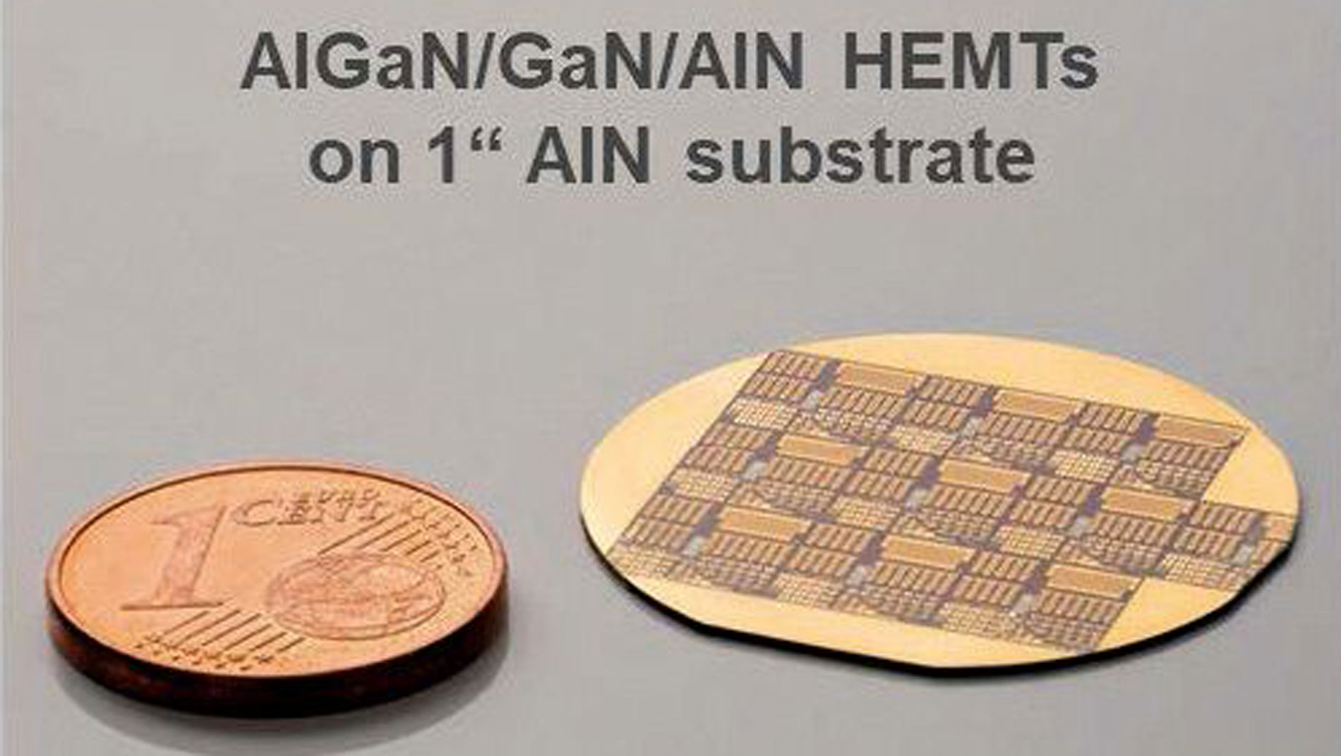
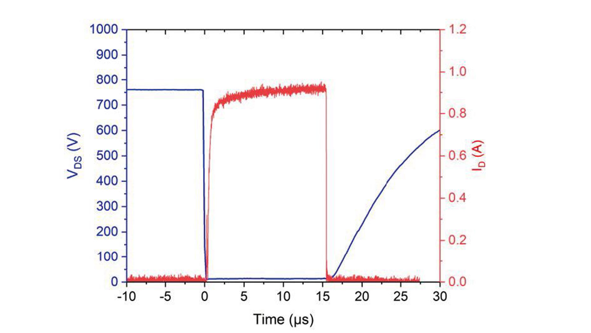
FBH has demonstrated AlGaN/GaN/AlN HEMTs on AlN substrates (Fig. 1), which show an average breakdown voltage scaling of 125 V/µm and a power figure-of-merit of VBr/(RON*A) = 1.17 GW/ cm² [3]. These are record values for high-voltage GaN channel transistors on AlN substrates. More than 2200 V breakdown voltage has already been achieved. The applicability of this technology for high-voltage power conversion was demonstrated with wafer-based 1 A switching transients up to 760 V [4], see Fig. 2. Here, the almost ideal AlN-substrate electrical isolation is essential to extend the AlN-based device technology towards monolithically integrated power-ICs for applications > 600 V.
To explore the benefits of the lateral AlGaN/GaN/AlN HEMT approach for monolithic integration at high voltages, FBH also grows this material stack on 4-inch semi-insulating SiC substrates. A drift zone breakdown voltage scaling of 140 V/µm has been achieved, which is approximately 20 % higher than for conventional GaN HEMT devices. Using this approach, transistors with 1790 V breakdown voltage have been realized. The resulting power figure-of-merit reaches 2.4 GW/ cm², surpassing that of most lateral GaN-based devices.
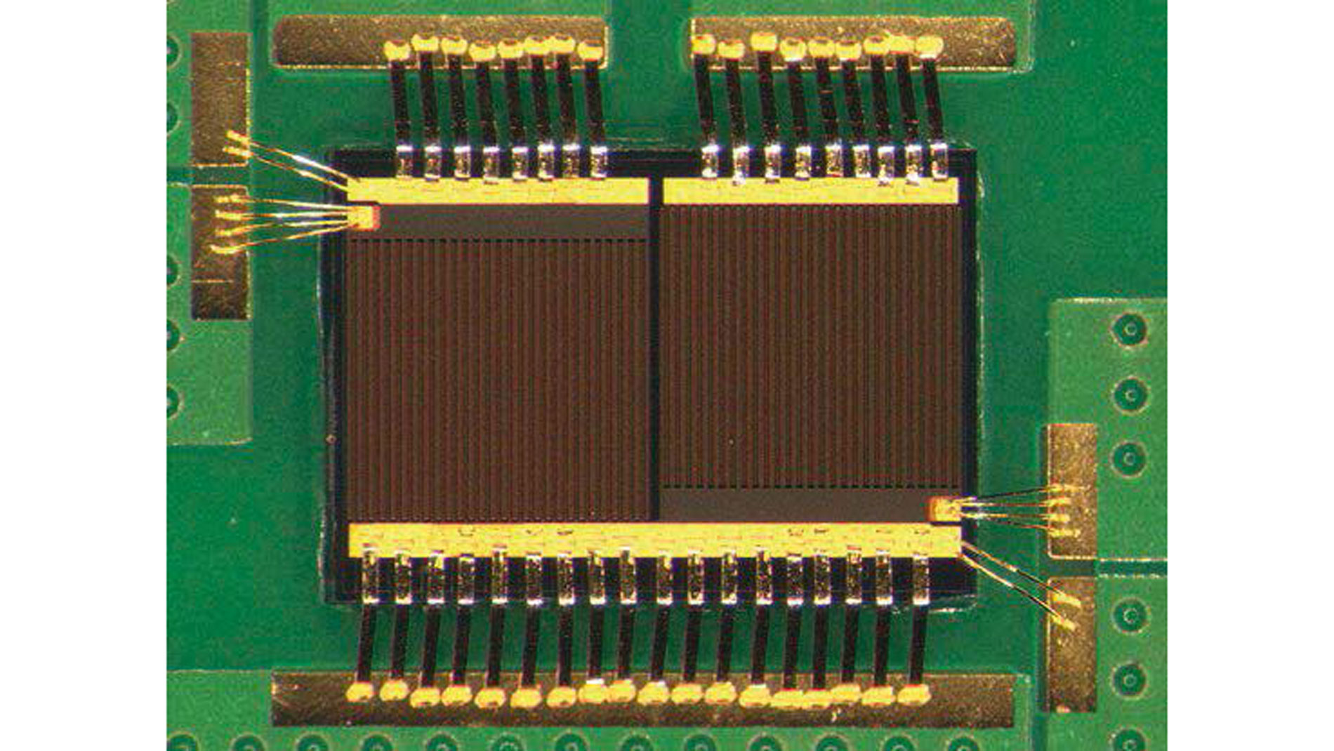
The 4-inch wafer size provides sufficient processing yield and chip area to realize monolithic half-bridges and bi-directional transistors without being hampered by back-gating losses during operation above 150 V. Such AlN-based power ICs reduce parasitic wiring inductances in both the switching-cell power loop and the gate-driving loops. And they are the key to benefit from the particularly high device switching speed on system level. Power converters can operate at higher switching speed, converter volume and mass can be reduced. Using his AlN-on-SiC platform, FBH’s power-electronics partners at Technische Universität Berlin (TU Berlin) have demonstrated 200 V/5 A hard-switching operation at 5 MHz with an integrated 2x120 mΩ half-bridge (Fig. 3) and +/-200 V/6 A T-type converter operating at 2 MHz with an integrated 120 mΩ bidirectional transistor [5].
Material for future power transistor generations: gallium oxide
Gallium oxide (β- Ga₂O₃) is a second semiconductor candidate for efficient power-electronic switches. The ultrawide-bandgap semiconductor possesses a bandgap of 4.8 eV. With an estimated dielectric strength of 8 MV/cm, it has the potential to drastically reduce the gate-to-drain distance with respect to SiC and GaN-based devices, thus allowing to fabricate more compact and efficient transistor devices with reduced switching and conduction losses. Therefore, FBH has launched research activities in recent years and joined forces with the Leibniz Institute for Crystal Growth (IKZ) to develop and process lateral and vertical Ga₂O₃ power switching transistors based on β-Ga₂O₃ substrates and crystals grown with the particularly cost-efficient Czochralski method at IKZ.
Lateral design – fast and highly efficient next-generation switching devices
FBH has successfully fabricated lateral Ga₂O₃-based transistor devices using active Ga₂O₃-semiconductor layers grown by MOCVD at IKZ on still very small 10×10 mm² epi-wafers, featuring a gate periphery of 10 mm. These MOSFETs reached 1800 V breakdown voltage and 2.5 A maximum drain current. In collaboration with TU Berlin, FBH has also demonstrated – for the first time – fast 400 V hard-switching transients with such devices enabling a 78 V/ns turn-off slope [6]. These results along with the measured high breakdown strength of 2 MV/cm emphasize the high potential of Ga₂O₃ for realizing fast and highly efficient next-generation power switching devices.
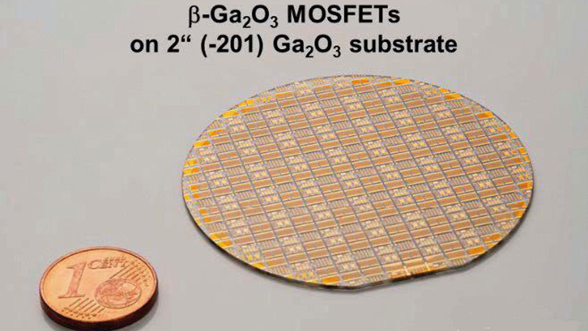
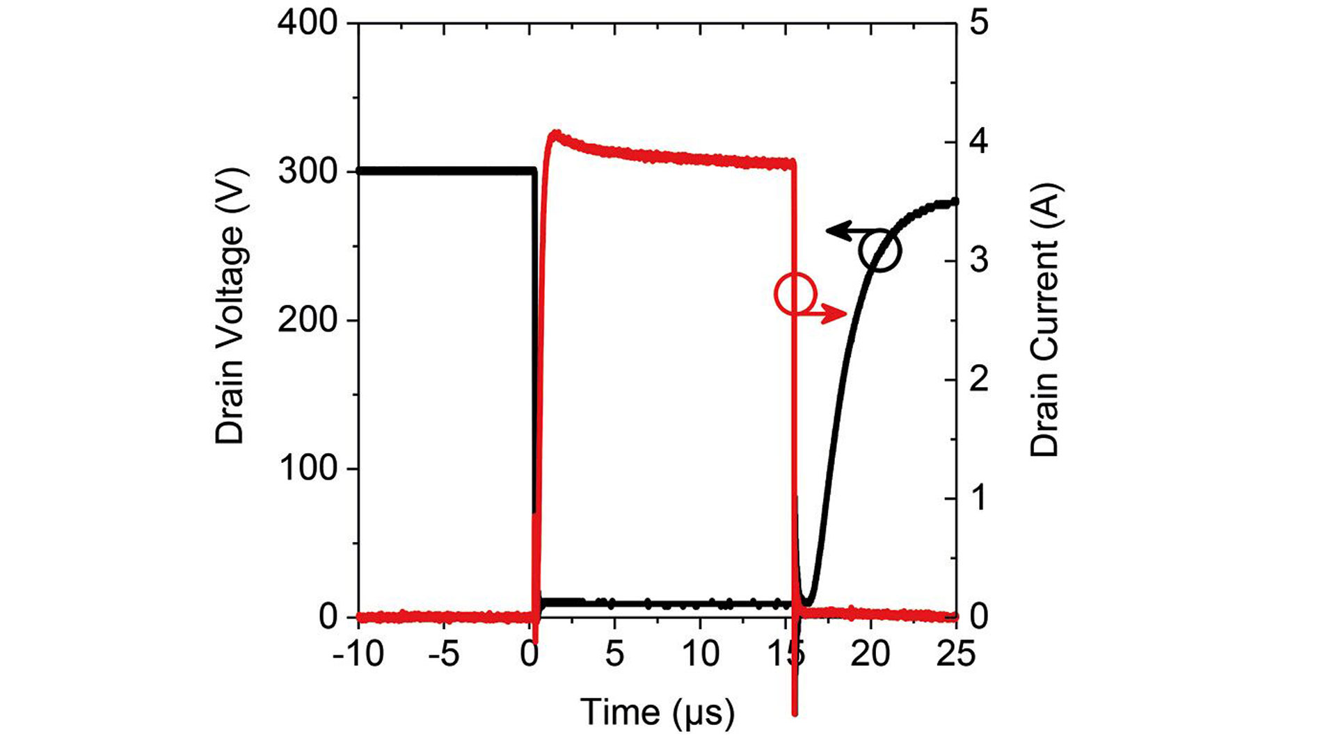
Device processing on larger wafers is essential for realizing power-electronic switches with on-state resistances < 1 Ω. To achieve this, FBH uses an implantation/activation approach to obtain the required n-type semiconductor structures inside a commercial insulating 2-inch Ga₂O₃ substrate (Fig. 4). The resulting Ga₂O₃ MOSFETs with 92 mm gate periphery have 750 mΩ on-state resistance and exhibit more than 10 A drain current. 300 V/4 A switching transients could be demonstrated [7], see Fig. 5. These reported Ga₂O₃ transistors feature the highest drain currents and blocking voltages under switching conditions so far published. Such results are crucial for assessing the competitiveness of Ga₂O₃ switching devices in power conversion in comparison with established SiC and GaN technologies.
Vertical design – optimal for future high-voltage, high-current applications
To fully exploit the material advantages of β- Ga₂O₃ in high-voltage, high-current applications, a vertical device structure is advantageous for active devices. This has already been widely demonstrated for vertical β-Ga2O3 Schottky barrier diodes. Main advantages include the smaller chip area at high voltage levels, the ideal separation of high-voltage potentials, improved reliability, and thermal performance as well as the potential to reach higher current levels. Most importantly, the FinFET topology allows for strong electrostatic gate control due to double gating of the channel at each fin structure. These characteristics enable enhancement-mode operation, making this structure very attractive for future high-power electronic applications.
Very recently, FBH has realized the first vertical β- Ga₂O₃ FinFETs, demonstrating enhancement-mode properties and an average breakdown strength up to 2.7 MV/cm [8]. This value already significantly exceeds the breakdown fields previously measured in FBH’s lateral β- Ga₂O₃ devices, despite the lack of edge termination in this initial design. These results emphasize the high potential of vertical Ga₂O₃ transistor architectures for future high-power electronic applications. (st)
References
- [1] H. Ahmad, Z. Engel, C. M. Matthews, S. Lee, W. A. Doolittle; Realization of homojunction PN AlN diodes. J. Appl. Phys. 7 May; 131,17, 175701 (2022). DOI: 10.1063/5.0086314
- [2] T. Kumabe et al., »Demonstration of AlGaN-on-AlN p-n Diodes With Dopant-Free Distributed Polarization Doping«, IEEE Transactions on Electron Devices, vol. 71, no. 5, pp. 3396-3402 (2024) DOI: 10.1109/TED.2024.3367314.
- [3] M. Wolf, F. Brunner, C. Last, H. Halhoul, D. Rentner, E. Bahat Treidel, J. Würfl, and O. Hilt, »1.17 GW/cm² AlN-Based GaN-Channel HEMTs on Mono-Crystalline AlN Substrate«, IEEE Electron Device Lett., vol. 45, no. 6, pp. 1048-1051 (2024), DOI: 10.1109/LED.2024.3391397
- [4] H. Halhoul, M. Wolf, F. Brunner, S. Besendörfer, M.D. Cuallo, S. Breuer, G. Lukin, A. Lesnik, E. Meissner, O. Hilt, »Beyond 650 V Dynamic Switching of High Voltage AlGaN/GaN/AlN HEMTs on Monocrystalline AlN Substrates«, 37th International Symposium on Power Semiconductor Devices and ICs (ISPSD), Kumamoto, Japan, Jun. 1-5, GaN1-05 (2025), DOI: 10.23919/ISPSD62843.2025.11117262
- [5] X. Geng, M. Wolf, C. Kuring, N. Wieczorek, O. Hilt, and S. Dieckerhoff, »Characteristics and Operation of a Monolithic Bidirectional GaN-on-AlN/SiC Power Transistor Employing Dual-Gate«, IEEE Trans. Power Electron., vol. 40, no. 4, pp. 5231-5240 (2025), DOI:10.1109/TPEL.2024.3516384
- [6] J. Böcker, K. Tetzner, S. Heucke, O. Hilt, E. Bahat-Treidel, S. Dieckerhoff and J. Würfl, »Dispersion effects in on-state resistance of lateral Ga₂O₃ MOSFETs at 300 V switching«, Electron. Lett., vol. 56, no. 16, pp. 838-840 (2020), DOI: 10.1049/el.2020.1286
- [7] K. Tetzner, H. Halhoul, M.D. Cuallo, and O. Hilt, »4 A/300 V Switching of Lateral β- Ga₂O₃ MOSFET Devices«, IEEE Electron Device Lett., vol. 46, no. 9, pp. 1601-1604 (2025), DOI 10.1109/LED.2025.3590836
- [8] K. Tetzner, M. Klupsch, A. Popp, S. Bin Anooz, T.-S. Chou, Z. Galazka, K. Ickert, M. Matalla, R.-S. Unger, E. Bahat Treidel, M. Wolf, A. Trampert, J. Würfl, and O. Hilt, »Enhancement-mode vertical (100) β- Ga₂O₃ FinFETs with an average breakdown strength of 2.7 MV cm-1«, Jpn. J. Appl. Phys., vol. 62, no. SF, pp. SF1010 (2023), DOI:10.35848/1347-4065/acbebc