UWBG semiconductors are the focus of intensive research due to their fundamental physical advantages over established materials such as silicon, silicon carbide (SiC) and gallium nitride (GaN). The key factor is their significantly wider bandgap, which leads to a much higher critical electric field strength. This enables components to operate at higher voltages while the drift zones remain thin. This significantly reduces turn-on resistance and conduction losses, enabling higher efficiency.
Another advantage is high-temperature resistance: UWBG materials exhibit lower leakage currents and remain stable under thermally demanding conditions. This opens up applications in environments where conventional semiconductors are unable to perform. The high electric fields and associated higher power density also allow for more compact and efficient systems, for example in power electronics for energy supply, electric mobility, and industrial drives.
UWBG semiconductors also offer new possibilities in the field of optics, as they can generate or process light in the deep UV range. This opens up applications in sensor and medical technology, as well as quantum research, which are only possible to a limited extent with existing materials.
The high level of research activity is therefore based on the potential to significantly enhance the efficiency and performance of electronic and optoelectronic systems. However, UWBG technologies are still in the early stages of development, meaning issues regarding material quality, heat dissipation, and integration into existing manufacturing processes remain subjects of intensive investigation.
Gallium oxide (Ga2O3) is considered a promising UWBG material as it has a particularly large bandgap (approximately 4.8 eV), giving it a very high critical electric field strength. This enables the production of components for very high voltages with comparatively low losses. Another advantage is the possibility of manufacturing Ga2O3 on large-format, cost-effective substrates, offering long-term economic benefits. However, this material presents a fundamental problem in that it has comparatively low thermal conductivity, placing very high demands on thermal management.
Ga2O3
Gallium oxide (Ga2O3) is considered a promising UWBG material due to its particularly large bandgap (approximately 4.8 eV) and consequently high critical electric field strength. This enables the production of components for very high voltages with comparatively low losses. Another advantage is that Ga2O3 can be manufactured on large-format, cost-effective substrates, offering long-term economic benefits. However, this material presents a fundamental problem in that it has comparatively low thermal conductivity, placing very high demands on thermal management.
High PC values alone are not enough
In their presentation, researchers from the University of Hong Kong highlighted the high PC values (switching power capacity, or the product of switching current and voltage) already demonstrated for UWBG devices, which reach into the kilowatt range. However, Hehe Gong and Xin Yang also emphasised in their presentation that the performance achieved so far is insufficient for industrial requirements. They explained: »Power modules in automotive powertrains typically require a rated voltage of 400 to 800 V and a rated current of 200 to 400 A, so to increase the PC value, power modules with multiple chips are crucial.« The absence of any power modules based on UWBG devices to date is attributed to the challenges in package design.
These must withstand very high electric field strengths while managing high heat fluxes and thermomechanical stresses simultaneously. In the case of Ga2O3, the aforementioned problem of low thermal conductivity is also a factor. One approach to overcoming these limitations is the so-called Junction-Side-Cooling (JSC) packaging technology; however, this often leads to a deterioration in breakdown voltage (BV). This is due to the unavoidable overflow of the die-attach material from the active region into the edge regions, which can result in localised heating.
Gong and Yang addressed this precise problem by developing a UWBG power module through joint electro-thermo-mechanical co-optimisation at the device and package levels. They tested two new approaches to solve the aforementioned problem. The paper states: »To preserve the BV, we introduce two interface designs between the device surface and the die attach: a post interface and a high-κ dielectric interface. These designs improve both device and package performance.’
These two designs both enable low thermal resistance (R_(Th)) via the JSC and reduce thermo-mechanical stresses by providing either a mechanical buffer or an improved CTE match. These benefits have been demonstrated through thermal resistance measurements and power cycling tests. Of these two designs, the high-κ interface was found to enable a 20% higher BV and a 50% lower RTh than the post design. Using the high-κ interface package, we assemble a six-die power module and demonstrate 1000 V, 200 A continuous switching in practical converters.«
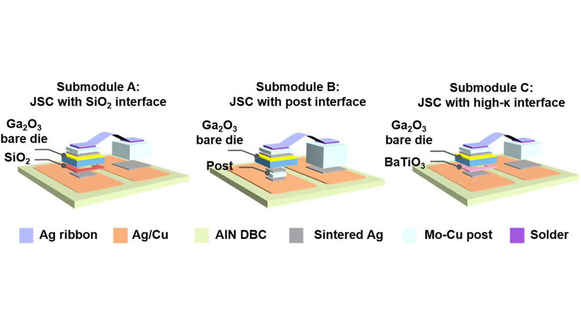
The researchers have developed three submodules in total, each utilising a different packaging architecture for a single Ga2O3 component. All three submodules are mounted directly onto a copper DBC substrate using flip-chip technology, which enables efficient junction-side cooling (JSC). The difference lies in the interface between the device and the housing. The first submodule (Submodule A) uses a conventional 100 nm-thick SiO2 insulating layer. The second submodule (Submodule B) uses a 500 µm-thick Mo-Cu post to mechanically separate the chip surface from the die-attach material. The third submodule (Submodule C) uses a 100 nm-thick BaTiO2 layer instead of the SiO2 insulating layer. This layer is inserted between the edge termination of the device and the sintered silver spread beyond the intended area at the chip edges to reduce electric field peaks. Additionally, all variants utilise a lateral Mo-Cu stacker to relieve thermomechanical stresses within the chip.
The underlying diode described in the paper is a p-NiO/n-Ga2O3 heterostructure with a stepped edge termination (JTE) structure, enabling a more uniform field distribution. Depending on the variant, the fabrication process involves depositing thin dielectrics or integrating the post, followed by silver sintering processes. Finally, the six submodules are connected in parallel to form a power module with a symmetrical DBC structure to ensure uniform current distribution. Encapsulation is carried out using silicone gel.
Electro-thermal-mechanical optimisation
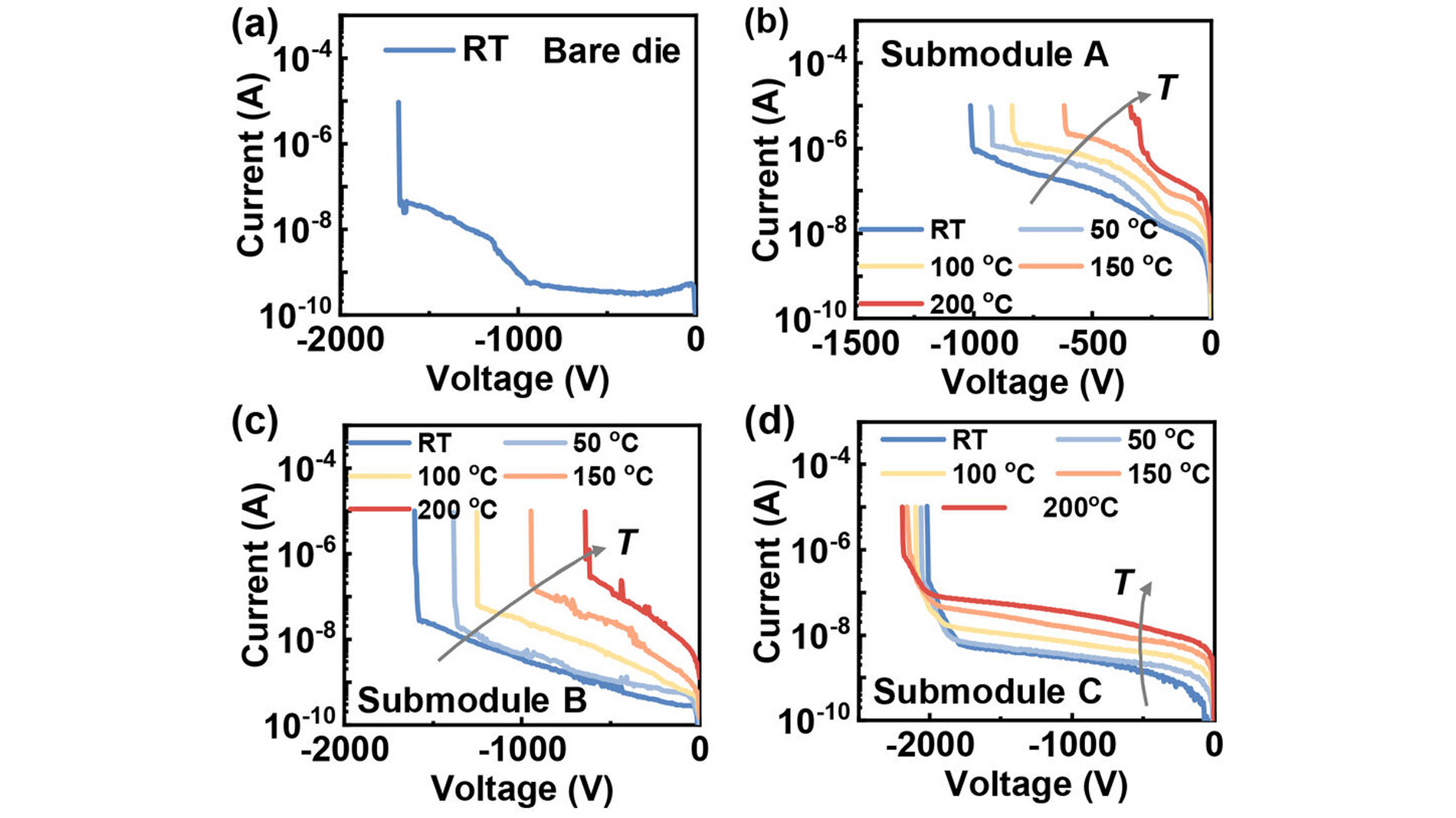
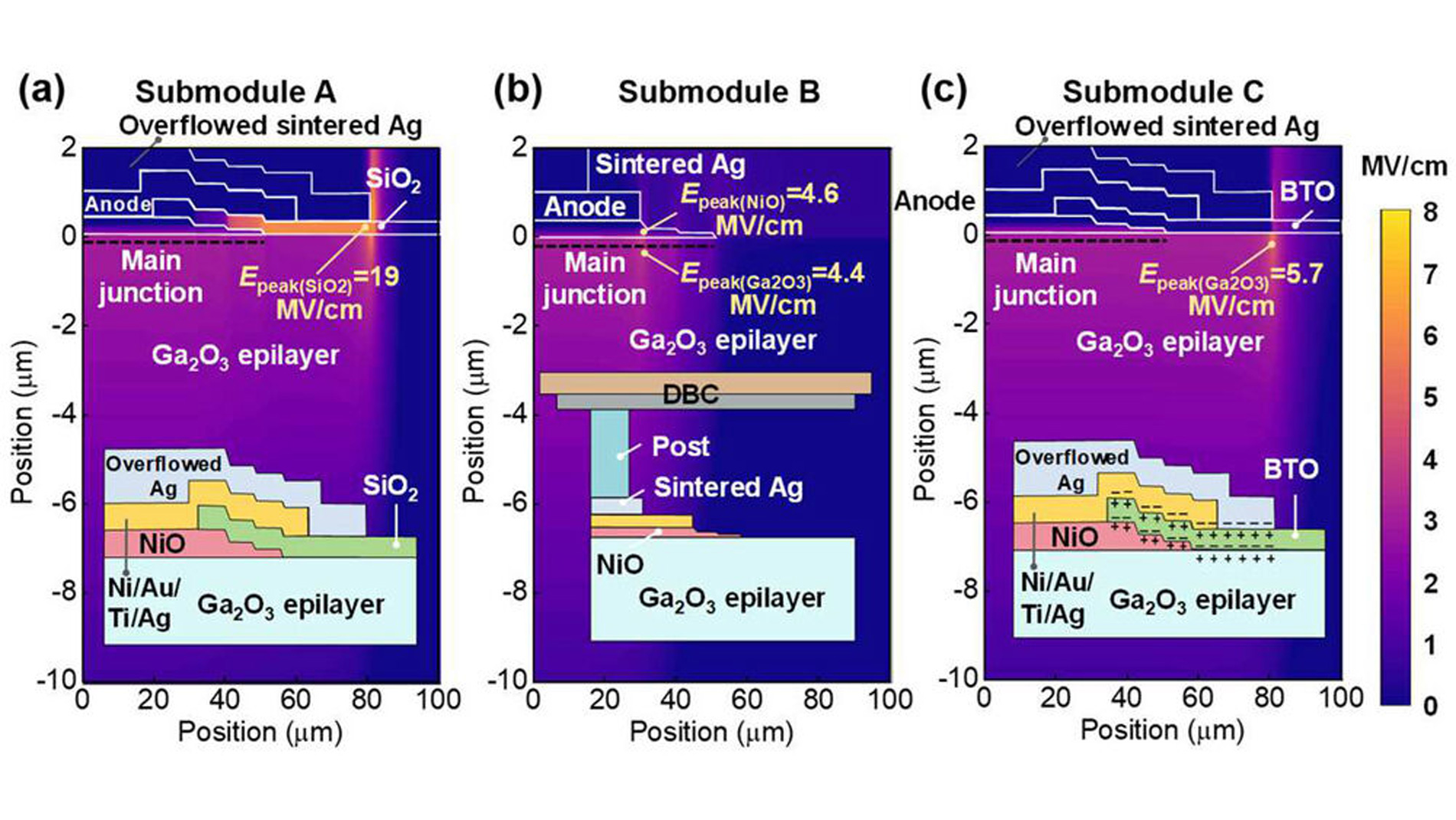
The I-V characteristics of all three submodules are temperature-dependent and exhibit similar behaviour, with the current-carrying capacity increasing as the temperature rises. However, simulations of the electric field distribution reveal significant differences. In submodule A, critical field peaks occur in the SiO2 layer; these are reduced by the post (submodule B) or the high-κ layer (submodule C). In particular, submodule C shifts the field peaks to the edge, achieving a higher breakdown voltage of up to 2 kV and improved behaviour at rising temperatures.
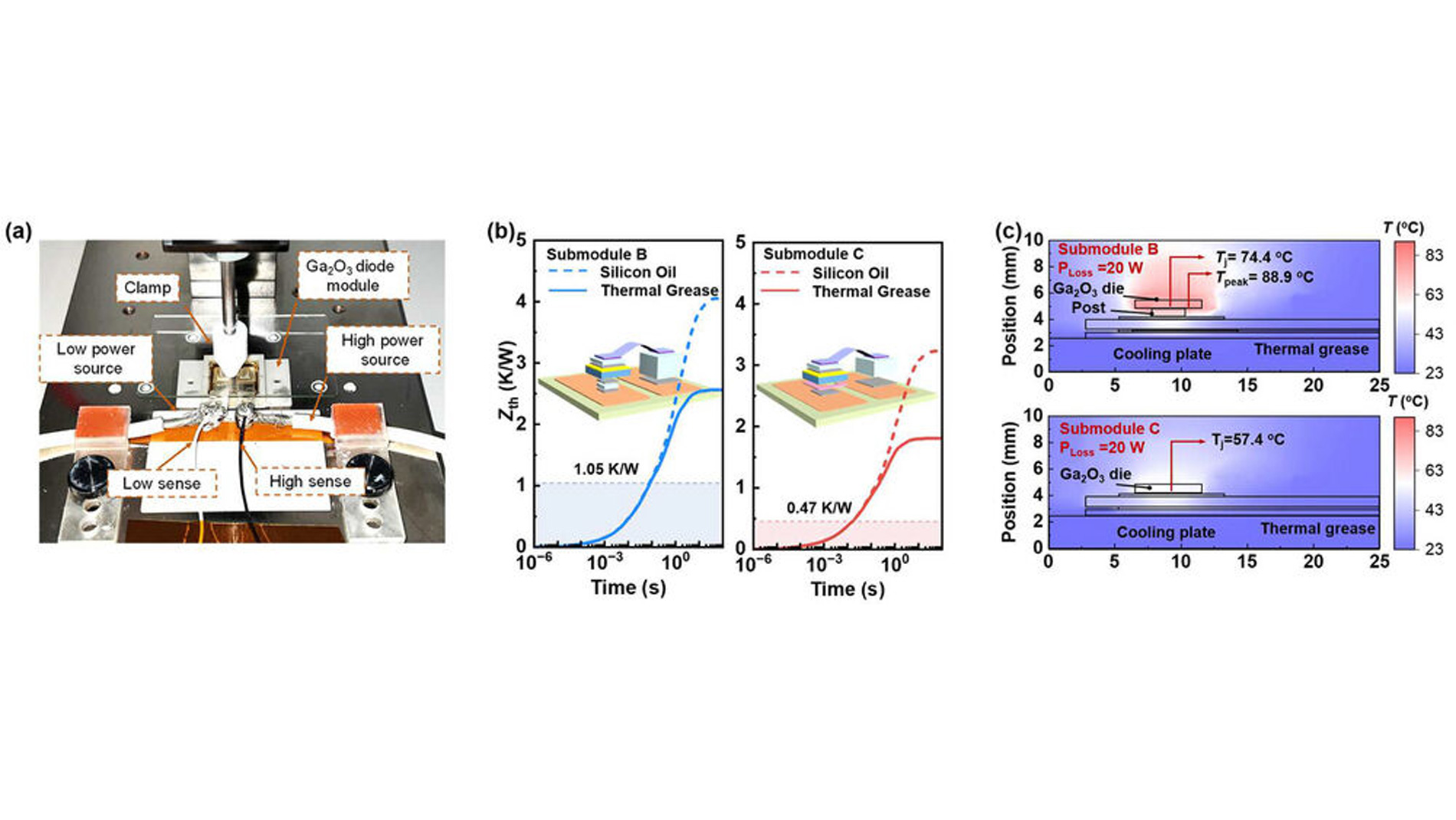
Thermal behaviour: Thermal characterisation shows that all submodules benefit from junction-side cooling and exhibit low thermal resistances. Submodule C achieves the lowest value of 0.47 K/W, which is a significant improvement on submodule B. The results confirm that heat is efficiently dissipated without flowing through the chip itself.
Mechanical properties: Differences are also observed in the thermomechanical stresses. Submodule A exhibits the highest stresses due to material incompatibilities. The high-κ layer in submodule C reduces these stresses by better matching the thermal expansion coefficients. The post in submodule B acts as an additional mechanical buffer, ensuring the lowest overall stresses.
Reliability: In power cycling tests, submodule A shows significant deterioration in electrical parameters, indicating material fatigue. In contrast, the properties of submodules B and C remain stable over many cycles, confirming their higher reliability.
Summary
A practical power converter was used to test the complete module, which comprises six Type C submodules. A turn-on time of 2.5 μs and a period duration of 1 ms were selected, corresponding to the operating profile of many pulsed power applications in areas such as power grids, medical technology and industrial plants. The measured switching waveforms revealed a switching voltage of 1000 V at a current of 200 A, and the near-absence of reverse recovery behaviour indicated low parasitic inductance in the module. Thermal imaging also revealed a uniform current distribution across all six submodules.
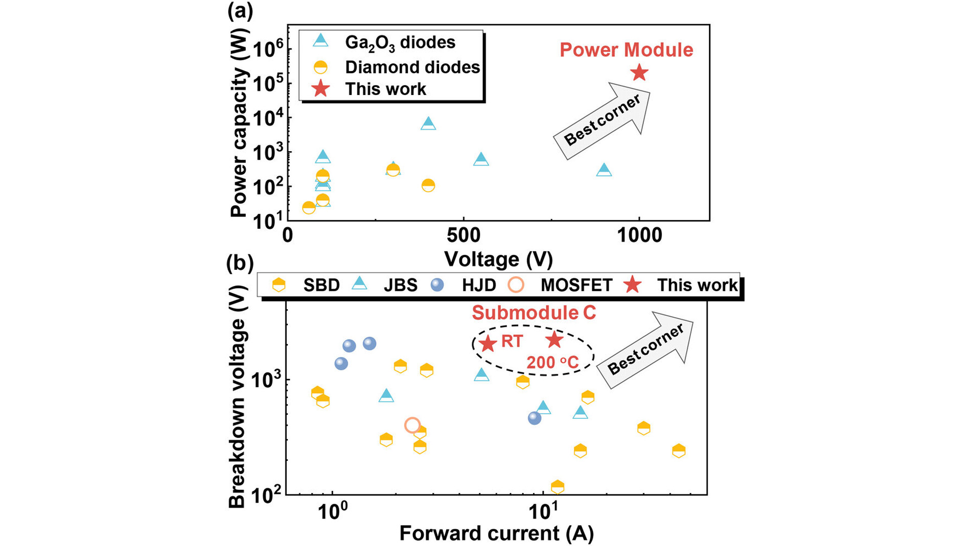
Comparing the switching voltage and power capacity (PC) with that of other published UWBG devices reveals an increase of around tenfold over the previous state of the art. Similarly, a comparison of the forward current and the breakdown voltage reveals that submodule C achieves one of the best combinations of a high current and a high reverse voltage.
In summary, the University of Hong Kong has, for the first time, demonstrated a UWBG power module with a power handling capacity of 200 kW. This breakthrough was achieved through the co-optimisation of the device and package in terms of electro-, thermo- and mechanics. The post- and high-κ interfaces both enable maintenance of the breakdown voltage, low thermal resistances, and reduction of thermomechanical stresses. In particular, the high-κ interface improves the breakdown voltage by 20% and reduces thermal resistance by 50%. These concepts can be transferred to various UWBG devices, opening up new possibilities for enhancing the performance of industrial applications. st