Infineon Technologies recently published its annual »GaN Insights 2026«. The report states that analysts expect the GaN power semiconductor market to reach almost $3 billion by 2030. This would represent growth of around 400 per cent compared to 2025. This growth is being driven by the ramp-up in production that has been underway since 2025, which is expanding the adoption of GaN across many industries and opening up new applications.
A compound annual growth rate (CAGR) of 44 per cent is forecast for the period from 2025 to 2030, with revenue expected to reach $920 million in 2026 — a 58 per cent increase on 2025. Furthermore »GaN is making inroads into numerous sectors, including AI data centres, robotics, electric vehicles, renewable energy, digital healthcare applications, and quantum computing. In data centres, GaN-based power supplies with new topologies are achieving unprecedented levels of efficiency and power density, reducing losses by up to 30 per cent and enabling more efficient, compact architectures. GaN-based motor drives in humanoid robots can be up to 40 per cent smaller, improving fine-motion control.«
So far, Ga-polar GaN has dominated practical RF applications
GaN is a polar material that is used, alongside other III-nitrides, in HEMTs (high-electron mobility transistors). Spontaneous and piezoelectric polarisation charges cause a two-dimensional electron gas (2DEG) to form at the heterojunction. The formation of this 2DEG, induced by polarisation effects and combined with high electron mobility and high saturation velocity, enables high current densities and fast switching.
»This makes GaN a key semiconductor material for high-frequency and millimetre-wave applications with high power and efficiency,« explained Umesh Mishra, Professor and Dean of the College of Engineering at UC Santa Barbara (UCSB), at this year’s ISSCC.
Due to polarisation, GaN has two polarity orientations that are used in HEMTs: Ga-polar and N-polar. The Ga-polar surface has a negative polarisation charge, while the N-polar surface has a positive polarisation charge. Mishra continues: »Initial research into GaN began with the Ga-polar orientation. The first HEMT was manufactured by APA Optics in 1993 and the first RF power GaN HEMT was realised at UCSB in 1996. Since then, further work based on several breakthroughs at UCSB, as well as in academia and industry, has led to remarkable improvements in the efficiency and output power of GaN.«
Research began with the Ga-polar orientation because it was much easier to achieve technologically and more stable. In epitaxial growth processes such as MOCVD, for example, Ga-polar GaN emerged as the preferred growth direction because thermodynamic conditions and nucleation layers favour this orientation. In contrast, N-polar growth was unstable for a long time and frequently resulted in a higher defect density. Ga-polar GaN also offered advantages in terms of surface chemistry and material quality. The surfaces are chemically more stable and less reactive, facilitating processing, and the early layers exhibited better crystalline properties. Furthermore, device physics is easier to utilise in Ga-polar HEMTs as polarisation effects directly lead to the formation of a stable 2DEG. Consequently, Ga-polar GaN HEMTs have become commercially established and are used in communications, defence and radar systems up to around 30 GHz, contributing significantly to the introduction of 5G.
N-polar GaN has been significantly less researched to date
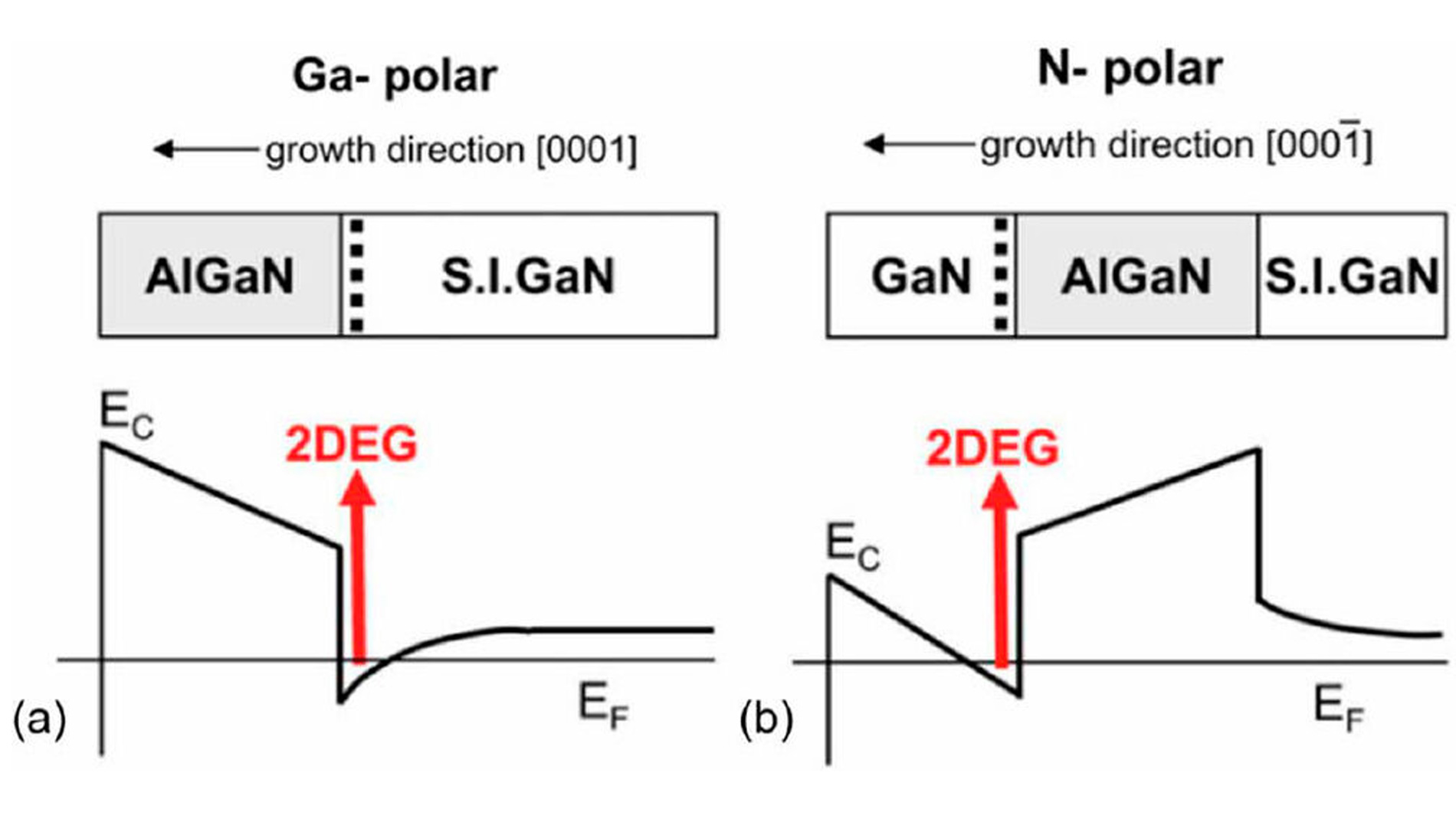
To date, N-polar GaN has received significantly less research attention than the Ga-polar variant. However, according to Mishra, it offers a wide range of possibilities for improving transistor performance due to the reversed polarisation fields – the fundamental difference between N- and Ga-polar orientation. The key difference lies in the arrangement of the barrier relative to the channel. In Ga-polar GaN HEMTs, the barrier is located above the channel. Consequently, a reduction in the gate-channel distance leads to a reduction in carrier density, and thus in current. This creates a fundamental trade-off between high gain and high output power. In contrast, in N-polar structures, the barrier is located below the channel. »This geometry allows the carrier density and the gate-channel distance to be adjusted independently, enabling high current densities, high output power, high gain and high efficiency to be achieved simultaneously,« says Mishra.
Another advantage of N-polar GaN is the use of a GaN cap layer in the source and drain regions. This increases conductivity in these regions and reduces the effects of charge carrier traps, which cause differences in DC and RF behaviour (DC–RF dispersion). These effects are more pronounced in Ga-polar GaN HEMTs, leading to lower power density and efficiency, particularly at millimetre-wave frequencies. According to Mishra, N-polar GaN enables virtually dispersion-free operation without current collapse or knee walkout (the shift of the knee point of the output characteristic to higher voltages due to charge carrier traps), and reduces memory effects (time-dependent effects caused by charge carrier traps where the behaviour of the device depends on its previous operating conditions). Mishra continues: »This enables the near-ideal behaviour of an RF power transistor with high output power, high efficiency, and good linearity. Accordingly, N-polar GaN HEMTs have so far been optimised particularly for applications in the W-band (75 to 110 GHz), where they have already demonstrated improved performance compared to Ga-polar structures.«
Various substrates
In current research, several substrates are being investigated for N-polar GaN, including silicon, GaN, SiC and sapphire. Each substrate has its own advantages and disadvantages in terms of cost, thermal conductivity, defect density, available wafer size, and lattice matching. Ideally, a substrate would be cost-effective, have high thermal conductivity, be available in large diameters and have a low defect density and a lattice constant that matches GaN well. Close lattice matching leads to fewer dislocations in the epitaxially grown layers, enabling improved device performance with reduced trap-induced effects. It also potentially allows for a reduction or elimination of the buffer layer thickness, thereby reducing thermal resistance at the transistor level. GaN substrates would be ideal under these conditions, but they are currently too expensive for mass production. As a result, sapphire and SiC have emerged as the most relevant substrates for RF GaN and N-polar GaN research. Sapphire offers a cost-effective solution with large wafer diameters and low defect density, enabling more economical devices and systems. SiC, on the other hand, provides significantly higher thermal conductivity, which is particularly advantageous for high-power applications.
Notably, the high efficiency demonstrated by N-polar GaN at 94 GHz improves the viability of sapphire substrates, as reduced power dissipation leads to lower thermal loads. In addition, emerging approaches such as integrating diamond layers in close proximity to the device can further reduce thermal resistance, making the choice of substrate less critical from a thermal management perspective.
N-polar GaN has great potential
Ga-polar GaN is now a key technology in the RF front end of modern communication systems, including 5G, satellite communications, and backhaul. However, as Mishra emphasises, N-polar GaN also has considerable potential to improve these systems further, particularly with regard to RF and millimetre-wave power amplifiers (PAs). Thanks to its higher power density and efficiency, N-polar GaN makes it possible to create more compact and cost-effective amplifiers. This is particularly significant for millimetre-wave applications, where the available power per amplifier is limited and phased-array systems are often required. According to Mishra, using highly efficient N-polar HEMTs enables such systems to be designed to be more compact, energy-efficient and lightweight, as there is less power dissipation and lower cooling requirements. These properties confer several key advantages on N-polar GaN HEMTs for modern communication systems:
- High power density at the transistor level: up to 8.8 W/mm (approximately three times higher than before).
- High efficiency (PAE): reduces energy consumption and heat generation, particularly in millimetre-wave applications.
- High power per antenna element: up to 1 W output power per transistor at 94 GHz, which is crucial for phased arrays despite the limited aperture.
- Good scalability to high frequencies (mm-wave and E/D-band): virtually constant power density of 8 W/mm in the range from 10 to 94 GHz.
- Enables compact, high-performance systems with fewer transistors and smaller circuits.
- Supports high-performance radio links over long distances, which is relevant for backhaul, satellite communications, and future mm-wave systems.
As output power increases, so does heat generation. This poses a key challenge, particularly for densely integrated systems and space-based applications, since heat can only be dissipated via radiation. However, according to Mishra, N-polar GaN can provide a solution, with record values of over 50% power added efficiency (PAE) in the W-band, as well as power densities of up to 8.8 W/mm and output powers of up to 1 W per transistor at 94 GHz. Mishra continues: »Although superior performance has so far been demonstrated mainly at frequencies above 75 GHz, N-polar GaN also has considerable potential for lower frequency bands due to its high breakdown field and high, dispersion-free current density combined with low output capacitance. This enables high output power and a greater Bode–Fano bandwidth than Ga-polar GaN.« Furthermore, a circuit based on N-polar GaN for frequencies above 100 GHz has recently been demonstrated for the first time. As load-pull measurement capabilities and drive power are limited in the D-band, the circuit was designed based on 94 GHz measurements and small-signal and pulse data for higher frequencies. To achieve this, a compact matching network was developed using coplanar waveguide technology. Despite being single-stage with no additional driver stage, the circuit achieved higher power density in the 120–150 GHz range than previous Ga-polar GaN-based circuits. Mishra concluded: »This demonstrates that N-polar GaN has great potential, both at the transistor level and in real high-frequency circuits.« st
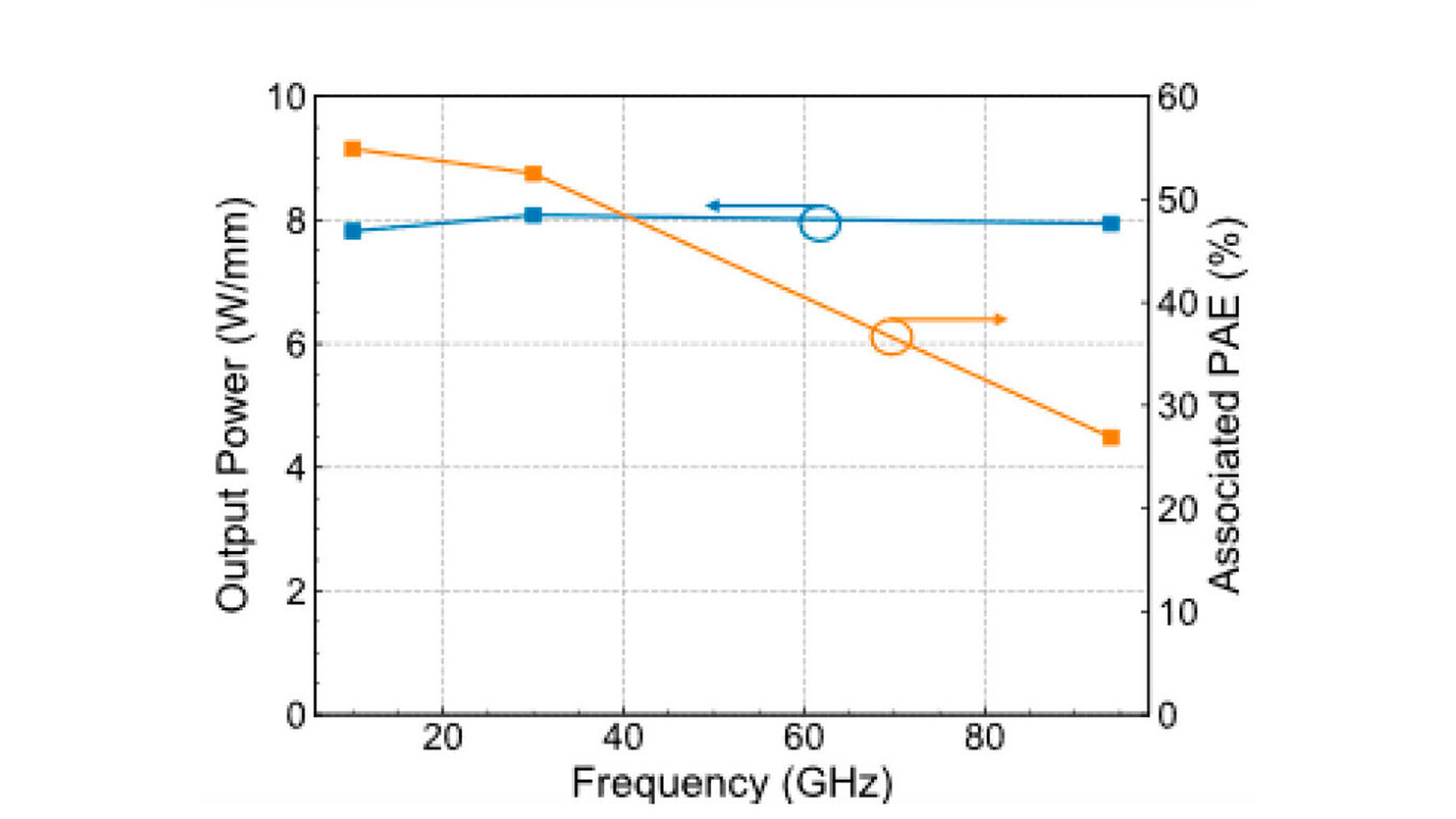
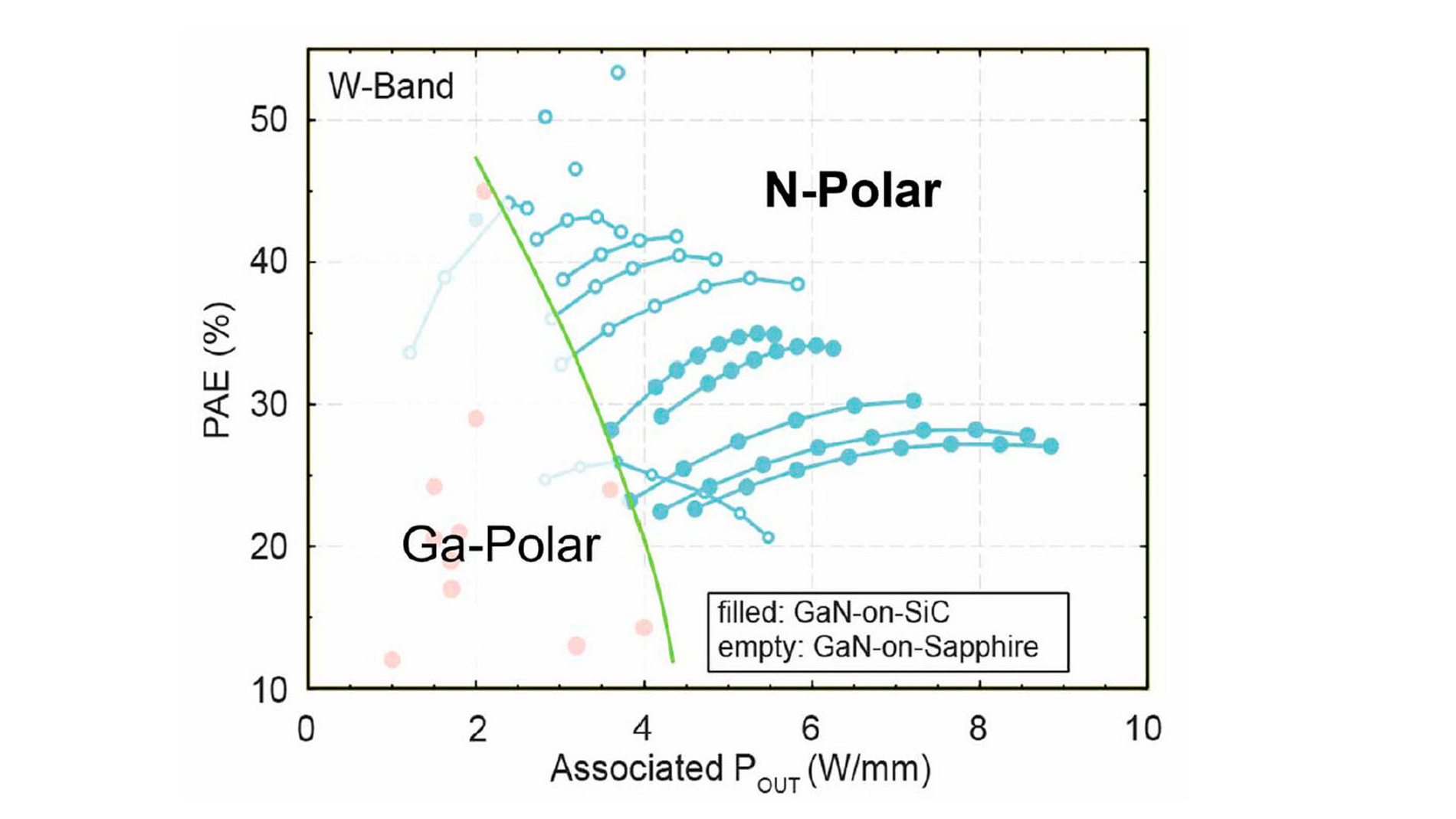
Figure 2: Demonstration of N-polar deep recess HEMTs having 8W/mm from 10-to-94GHz with a drain bias of 20V. Image: University of California, Santa Barbara
Figure 3: Comparison of peak PAE and its associated Output power in W/mm for N-polar and Ga-polar at W-band frequencies. N-polar shows a higher output power and PAE, illustrating its ability of obtaining larger breakdown fields than Ga-polar. Image: University of California, Santa Barbara