By Mathias Mahn, Business Development FAE, Vishay Europe
Introduction to Auxiliary Power Supplies
Auxiliary Power Supplies are used in various applications. They are usually used to power the internal low voltage circuits. Most commonly these are control circuits such as the microcontroller, biasing, colling fans or sensors. For this kind of circuitry usually only limited power is necessary. The overall consumption for most of the applications is assumed to be below 50 W.
Usually, these power supplies also require an isolation barrier. For such kinds of power supplies the flyback topology has proved to be a cost effective and simple solution. It is used in many applications with low to medium power requirements and different input voltages. A solar inverter is for example an application where a high voltage and wide range input is required. For inverters which need to work without grid power in island mode, the inverter needs to be supplied by the power coming from the DC input of the PV-string. Depending on the number of modules in the string and the ambient conditions this voltage can vary a lot. Practically the input voltages are somehow limited to approximately 200V to 1000V.
Also, the change in the mobility towards electric vehicles increases the demand for such power supplies. Common voltages used in the powertrains are now already at 800 V making it necessary to use such high voltage auxiliary power supplies in cars and the associated charging infrastructure.
Advantages of SiC MOSFETs
For high input voltage range power supplies a high VDS switch is required to ensure safe and reliable operation. Classical silicon MOSFET technology is limited in terms of high VDS. Common voltages for high voltage silicon MOSFETs are somehow limited to approx. 1kV. Moreover, at high voltages it offers poor performance in terms of RDSOn, leading to lower efficiency and higher losses. For designs with higher VDS requirements cascoded MOSFET designs could be an option. But this leads to a more complex and potentially more expensive design.
Wide bandgap semiconductors such as silicon carbide allow higher voltages making it possible to realize power supplies with a single MOSFET. This eases the design and reduces component count.
Also, the potentially high frequencies allow it to use smaller magnetics. Due to the lower conduction losses cooling effort is also less compared to classical solutions. These properties make them an ideal choice for such switching applications.
Realization of a Reference Design
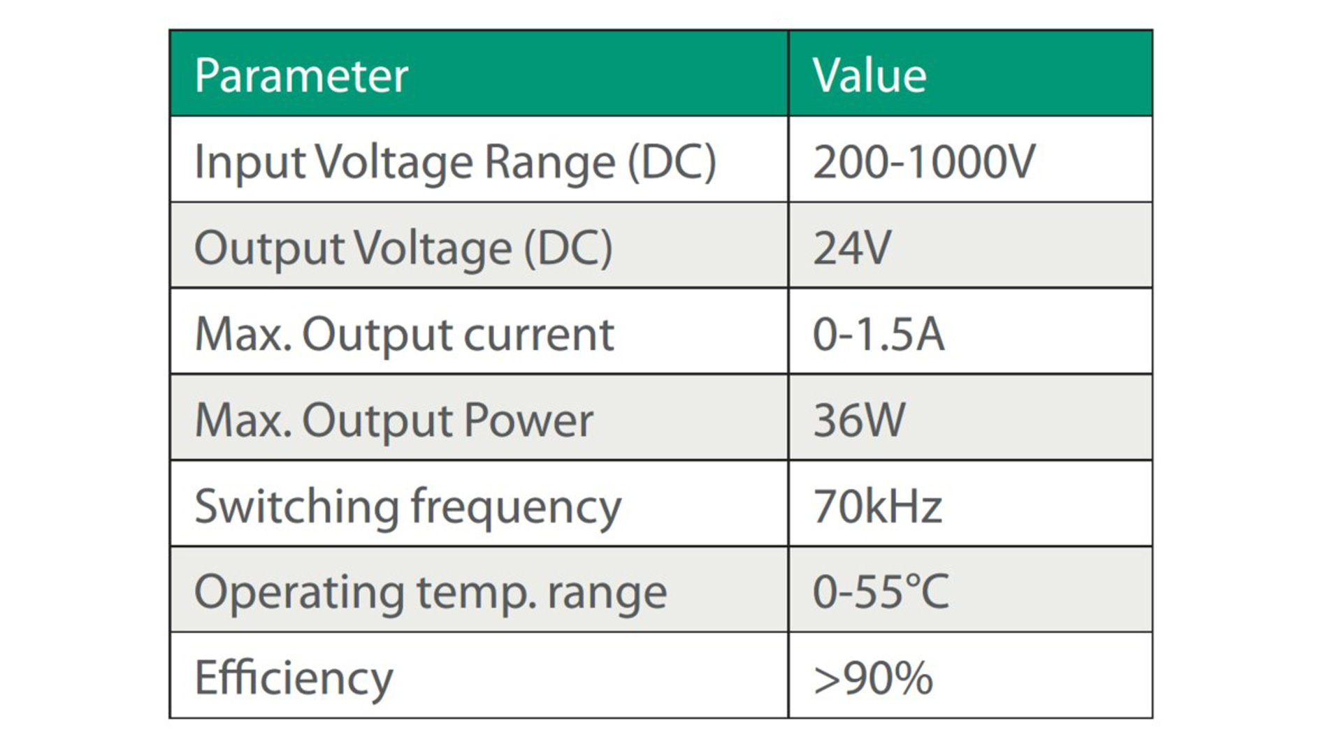
Vishay developed a reference design, targeting applications with high voltage wide range input requirements and low power consumption. The reference design is intended to show the advantages using SiC MOSFETs to simplify the design and provide a cost-effective and robust solution. In Table 1 the electrical parameters of the design are summarized and Figure 1 shows a simplified schematic.
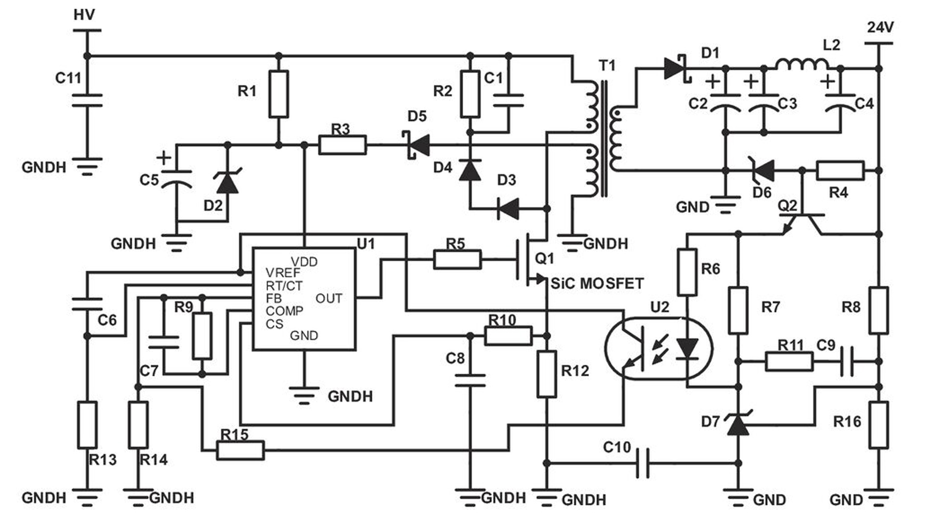
An important consideration is choosing the controller IC for the power supply. A large variety of different controllers allowing various operating modes and special features are available on the market from different vendors. For this design a Texas Instruments UCC28C58DR PWM controller was selected. This controller allows higher VDD voltages up to 30 V, giving greater flexibility in providing the necessary gate driving voltage for the SiC MOSFET. The IC is a current mode PWM controller for fixed frequency operation.
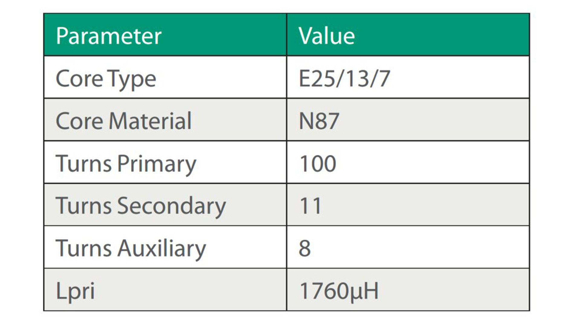
Another critical component of a flyback converter is the transformer. The parameters directly influence the overall system efficiency and power losses. The winding ratio and the parasitic parameters of the transformer influence the peak voltage, the SiC MOSFET needs to withstand. The RCD snubber circuit must also be designed according to the corresponding winding ratios and parasitic parameters to ensure enough safety margin for the SiC MOSFET. The winding ratio determines the output voltage of the converter and the auxiliary voltage to supply the controller IC. The selection of the winding ratio and inductance also influences the operating modes of the overall converter, operating either in CCM or DCM mode. Table 2 lists the Parameters of the used transformer made by Vishay Custom Magnetics.
For the switching MOSFET Vishay’s newest generation MXP170A560SE SiC MOSFET is used. This MOSFET has a maximum VDS of 1700 V, giving enough safety margin for this design. The MOSFET is manufactured with planar technology. For single switch applications the -5 VGS driving voltage for turn off is not required, so that the controller IC is sufficient for driving the MOSFET.
The high input voltage is also complicated for other components of the power supply. Although a big input capacitor is not required for the design, a small input DC link capacitor is placed at the input. Here a MKP1848 series foil capacitor is used which can handle voltages up to 1200 V. This avoids the use of several series connected aluminum capacitors which might require extra selection or even balancing. However, for some other parts of the design, it is necessary to use series connections of components to withstand the high voltages.
At the secondary side a 200 V Schottky diode is used for rectification. Although synchronous rectification would result in higher efficiency, the effect is considered to be negligible because of the relatively high output voltage and low currents. For the output capacitor Vishay’s broad portfolio of capacitor technologies made it possible to select from different capacitor technologies to obtain a small and low ESR solution. Here a combination of aluminum polymer and tantalum polymer capacitors is used.
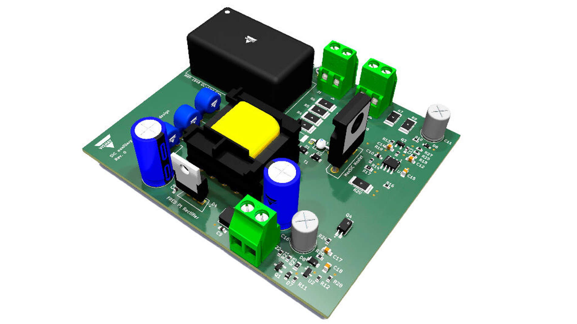
Loop compensation is realized with classical optocoupler feedback with a shunt regulator to achieve a fast loop response and stability. Figure 2 shows a 3D Model of the assembled PCB of the reference design.
The design was tested over the whole operating voltage range. It operates in Continuous Conduction Mode (CCM) with 200 V input voltage and 70 to 100 percent load. With increasing input voltage CCM operation is decreasing until it operates only in discontinuous conduction mode.
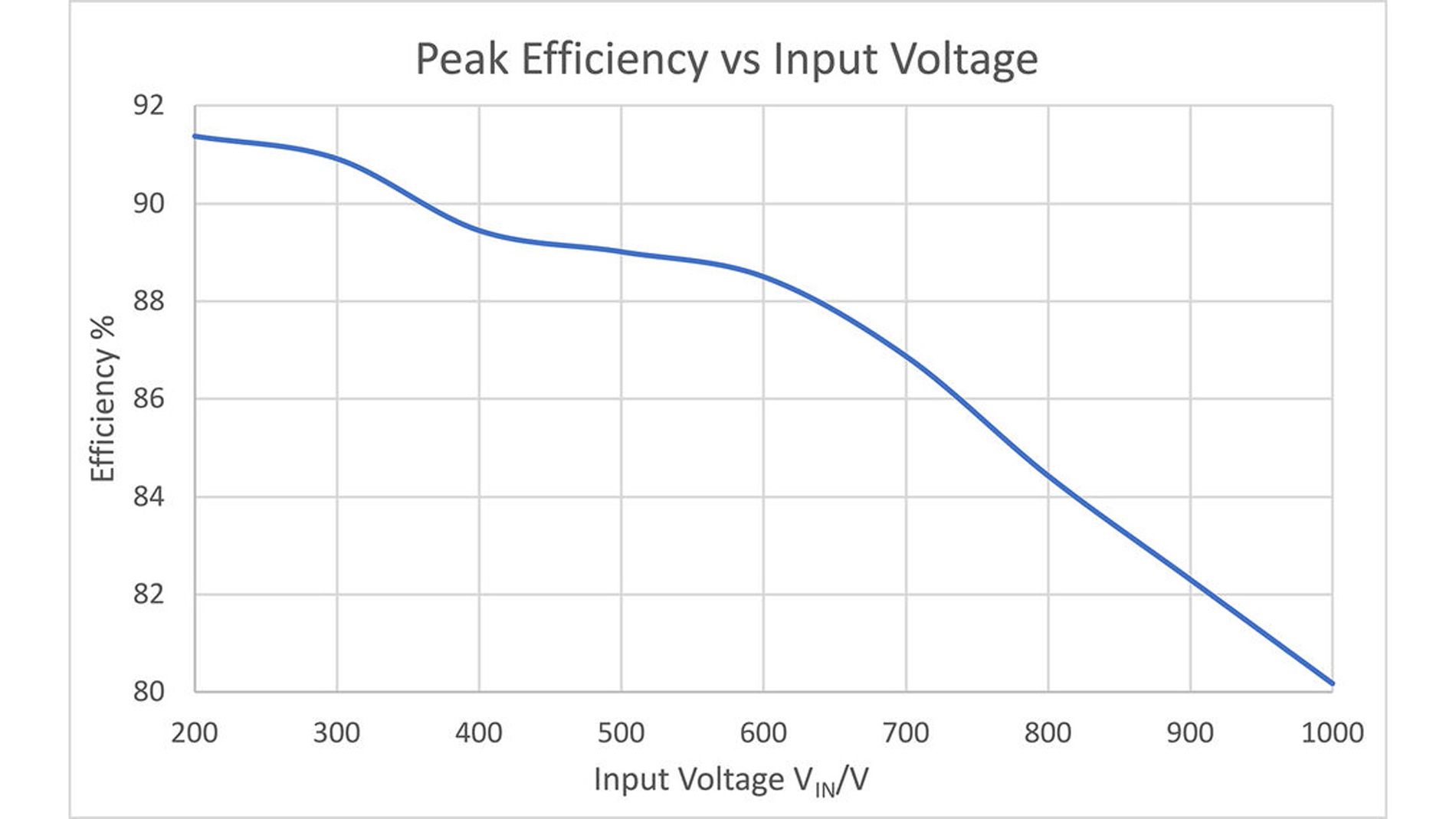
The drain source voltage remains always well below the rated 1,7kV of the SiC MOSFET showing the effectiveness of the RCD snubber circuit. Efficiency testing of the converter shows the expected behavior. Switching losses are increasing significantly with increasing output voltage. The peak efficiency is obtained at the lowest input voltage and is 91 percent.
With increasing output voltage, the efficiency drops to 80 percent at 1000 V input voltage at full load. Figure 3 shows the results over the whole voltage range.
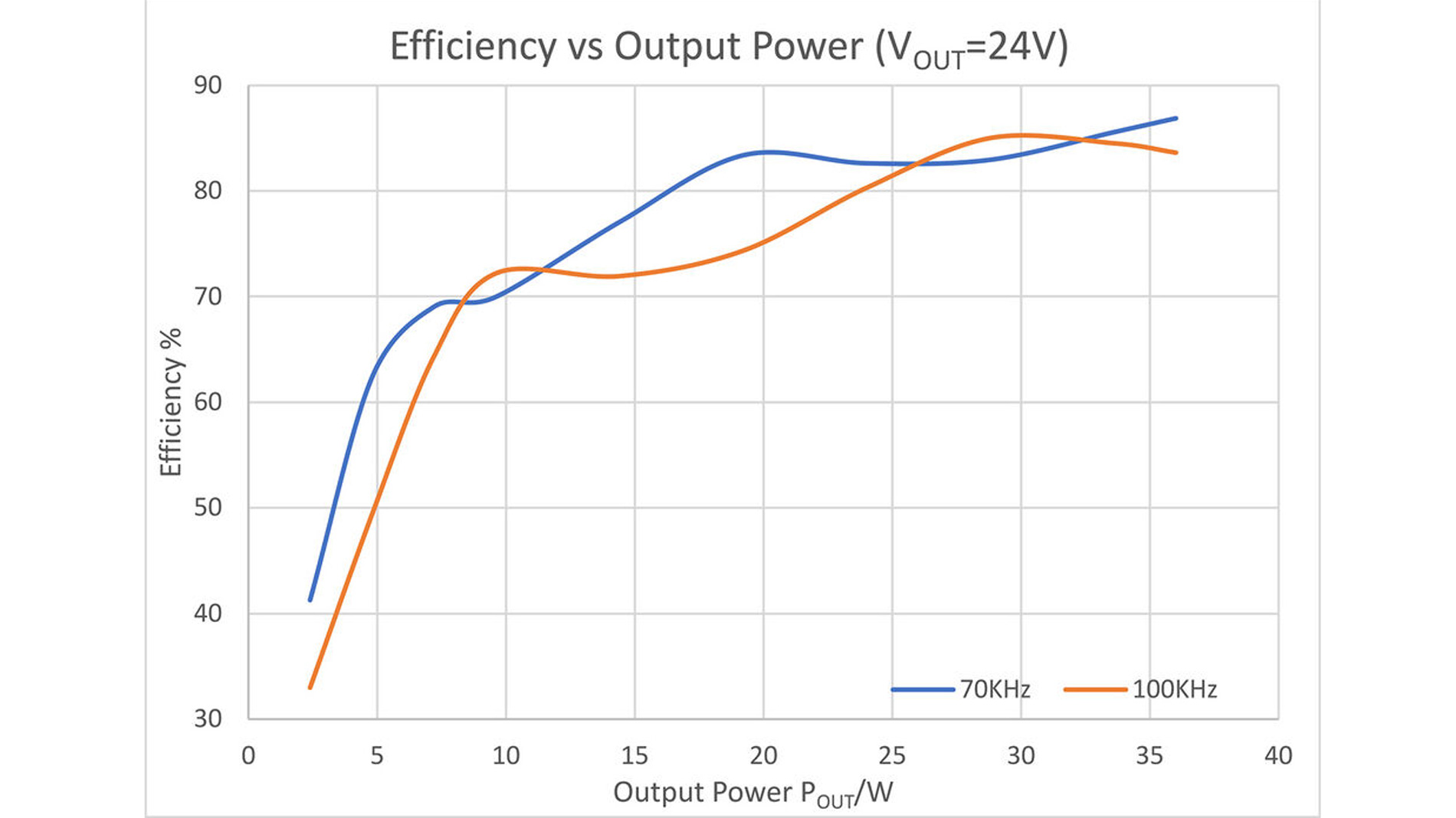
Also, a comparison between different switching frequencies was made. Usually, higher frequencies make it possible to use smaller magnetics. The problem is, with increasing frequency, skin and proximity effect become more important and require more complex magnetics. At a certain point it is hard to further reduce the size of the transformer due to these effects. In this design the switching frequency was set to be 70 KHz. The measurements showed no improvements with higher frequency. The biggest problem was here the temperature of the transformer which increased with increasing frequency. Figure 4 shows the efficiency curve for 70KHz and 100KHz operating frequency.
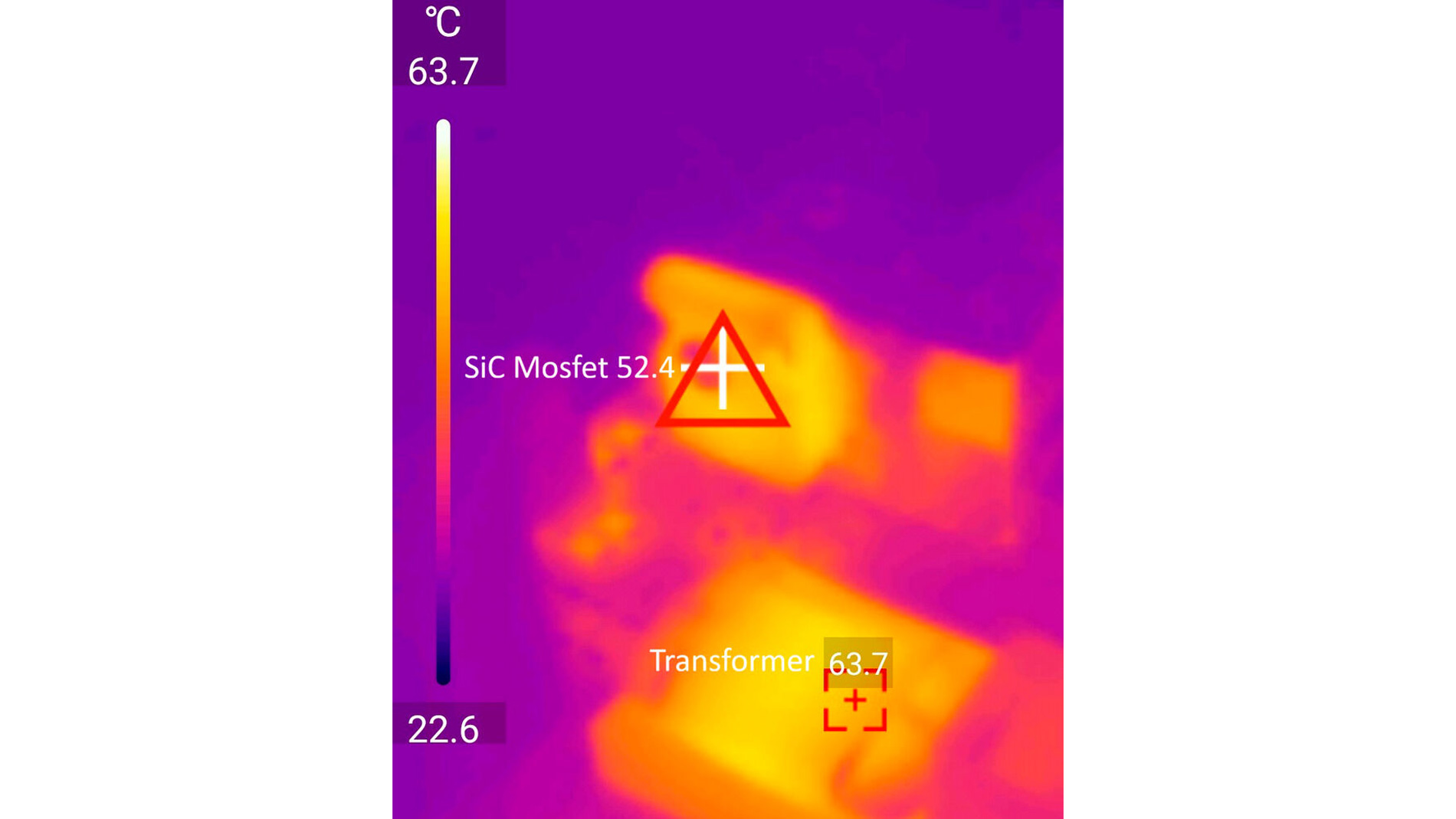
The Thermal measurements were also performed to validate that all components are well below their maximum operating temperature. The highest power dissipation for the design is expected at the maximum input voltage of 1000 V and full load. Tests were performed at this load scenario.
The primary side SiC MOSFET and the secondary side rectification diode are equipped with a small heatsink. Thermal measurements show that the temperature rise at the SiC MOSFET is 31 °C. The hottest component is the transformer with a temperature rise of 41,1 °C
Figure 5 shows the thermal performance at 1000 V input voltage and under full load. eg