The increasing demands on computing power, energy efficiency and power density in data centres are well known, simply because more data needs to be processed, transmitted and stored more quickly. This also increases power consumption – a GPU in a data centre, for example, can consume several hundred watts – which in turn creates thermal challenges. To meet these growing demands, advanced integration methods such as 3D packaging to increase system density, as well as new semiconductor materials such as GaN to improve efficiency and performance, are required. Traditional power supply architectures are increasingly reaching physical and architectural limits, as rising currents lead to higher conduction losses and more complex routing structures. At the same time, modern systems require ever closer coupling between the power supply and the computing unit.
In its presentation at IEDM 2025, Intel addressed the issue of power supplies for semiconductors in data centres, proposing an approach that would enable them to be integrated more efficiently and densely, and closer to consumers. This new approach is necessary because existing discrete voltage converters and silicon-based solutions are reaching their efficiency, size and power dissipation limits as power requirements increase. The 300 mm GaN-on-silicon technology offers significant advantages in this regard, as it boasts superior performance metrics compared to traditional silicon solutions while simultaneously enabling the integration of low-voltage to 48 V GaN devices with silicon CMOS. This creates a platform suitable for both power and high-frequency applications.
In his IEDM presentation, Han Wui Then, Senior Principal Engineer at Intel, highlights three unique innovations achieved by Intel: The industry’s thinnest GaN chiplet with an underlying silicon substrate just 19 µm thick; This chiplet was derived from a fully processed, thinned and singulated 300 mm GaN-on-silicon wafer, demonstrating outstanding transistor performance and excellent quality metrics.
The industry’s first library of fully functional, integrated on-die CMOS digital circuits ranging from inverters and logic gates to multiplexers, flip-flops and ring oscillators. These were realised using monolithically integrated GaN-NMOS and Si-PMOS processes; Promising results from TDDB, pBTI, HTRB and HCI studies, which suggest that 300 mm GaN MOSHEMT technology can meet the required reliability metrics.
Intel’s approach in detail
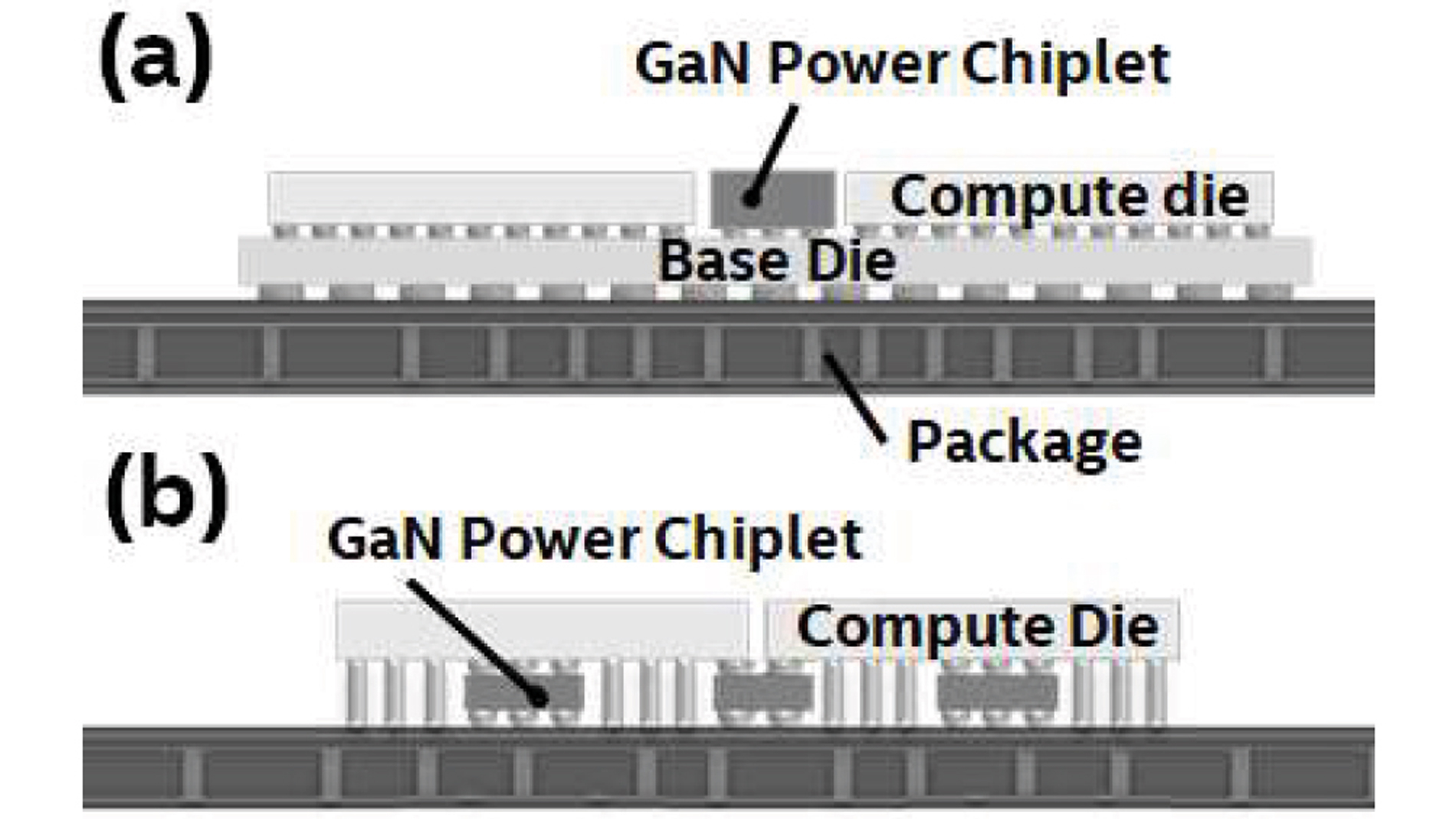
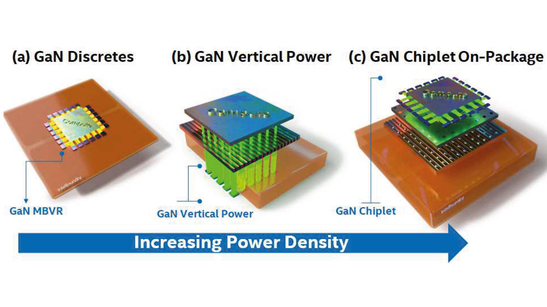
Against this backdrop, Then describes in his presentation the technological foundations for a scalable GaN chiplet architecture specifically tailored to the requirements of modern data centres. The objective is to bring the power supply closer to the load (point-of-load) to minimise line losses, particularly I²R losses, while significantly enhancing efficiency and power density. This integration takes place within the framework of advanced 3D packaging concepts, with GaN-based power chiplets embedded directly into the system. Intel also outlines the development trajectory from traditional discrete motherboard voltage regulators (MBVRs) to highly integrated, chiplet-based solutions. As demands on power density and efficiency increase, GaN-based power functions are being moved ever closer to the load and integrated directly into the package.
According to Then, a key challenge is that only very limited space is available within such highly integrated systems. Consequently, the GaN transistors used must offer high performance and integration density. Intel’s 300 mm GaN-on-silicon MOSFET technology achieves current densities of around 10 A/mm², and by scaling the gate length down to 30 nm it offers the potential for significantly higher current densities.
The GaN chiplets must also be extremely thin (less than 50 μm). The GaN chiplets presented by Intel are based on fully processed 300 mm GaN-on-Si wafers. The silicon substrate of these wafers is subsequently reduced to just 19 μm, after which the wafers are separated. This thinning and separation is carried out using the SDBG (Stealth Dicing Before Grinding) process, which enables stable mechanical processing despite the wafer’s extreme thinness. This thinness enables the creation of short, low-resistance through-silicon vias (TSVs), thereby reducing electrical losses and thermal resistance. Meanwhile, the performance of the transistors remains high: measurements show leakage currents of less than 3 pA/μm, stable characteristics at voltages up to 78 V and an excellent Ron-Qgg value of approximately 1 mΩ·nC.
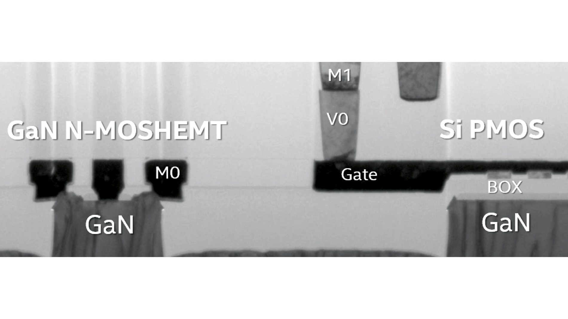
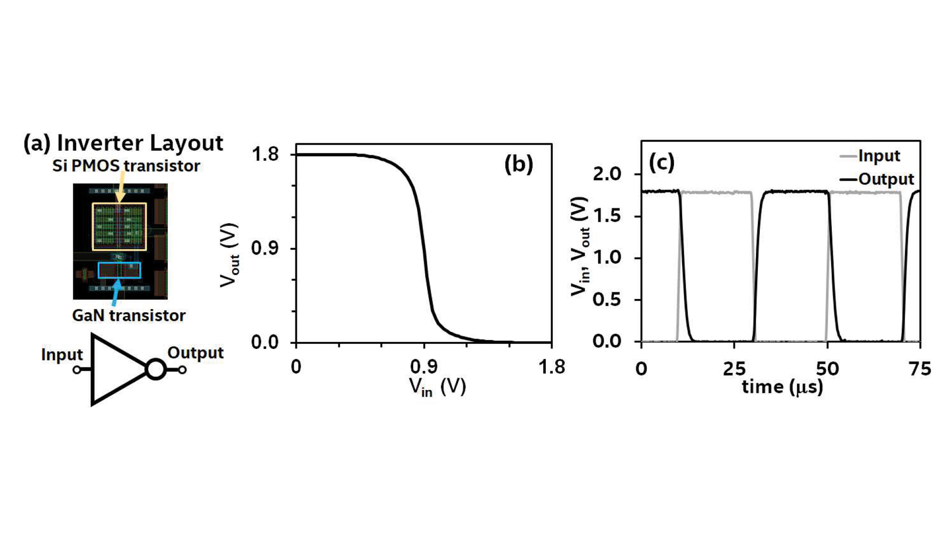
Another distinctive feature is that, as there is no space for separate CMOS companion dies in complex systems and connecting them would cause additional losses, Intel is pursuing a monolithic integration approach. In this approach, CMOS functionalities are implemented directly on the GaN chiplet. Alongside digital logic circuits, these integrated functionalities include the essential control and driver functions required for efficient switching and minimising passive components. For the first time, Intel has demonstrated a complete library of functional digital circuits, including inverters, logic gates, multiplexers, flip-flops, and ring oscillators. This is achieved by combining GaN-NMOSHEMT transistors with integrated silicon PMOS structures, applied using layer transfer. The measured circuits demonstrate high functionality and speed; for example, the delay of an inverter is around 33 ps.
Furthermore, GaN-MOSHEMT transistors demonstrate high performance in the high-frequency range. For a gate length of 30 nm, an fT/fMAX of 212/304 GHz is achieved, and a fMAX value of over 200 GHz is attained for gate lengths up to 130 nm. The RF data measured on the GaN chiplet are promising for RF and high-speed applications such as photonics, in Then’s view. The high cut-off and maximum oscillation frequencies highlight the potential of this technology for applications beyond pure power electronics. Then: ‘This GaN chiplet technology could potentially be used in such applications.’Another crucial aspect is the reliability of the technology. Intel has conducted extensive research into this area, including analyses of time-dependent dielectric breakdown (TDDB), positive bias temperature instability (pBTI), hot carrier injection (HCI), and high-temperature reverse bias (HTRB) testing. Overall, the results demonstrate stable transistor behaviour. For example, the TDDB analysis shows that the maximum operating voltage is 1.84 V for a ten-year lifespan at 90 °C, with a failure rate of 1 ppm.
pBTI and HTRB investigations show that the transistor parameters stabilise following an initial ‘burn-in’, with both the threshold voltage and the on-resistance becoming stable. HCI analyses also demonstrate high long-term stability, showing that the transistors can operate under realistic stress conditions for ten years. Then concludes: »These results show that a complete technological foundation for GaN chiplets on 300 mm wafers is now in place. The combination of ultra-thin chiplets, high power density, integrated CMOS functionality, and proven reliability represents a promising opportunity for high-density, high-power, and energy-efficient power electronics, as well as high-speed and RF applications«. st