By Peter Gergely and Andrej Kanovsky, onsemi Slovakia
Megawatt charging systems are designed to transfer large amounts of energy in short periods whilst supporting different vehicle and battery voltages. Modular architectures are well suited to this purpose, with the grid-side AC/DC conversion and the vehicle-side DC/DC conversion being functionally separated. The AC/DC stage generates a regulated DC intermediate circuit voltage, while subsequent DC/DC converters adapt this voltage to the respective vehicle battery.
Multiport architecture for megawatt charging
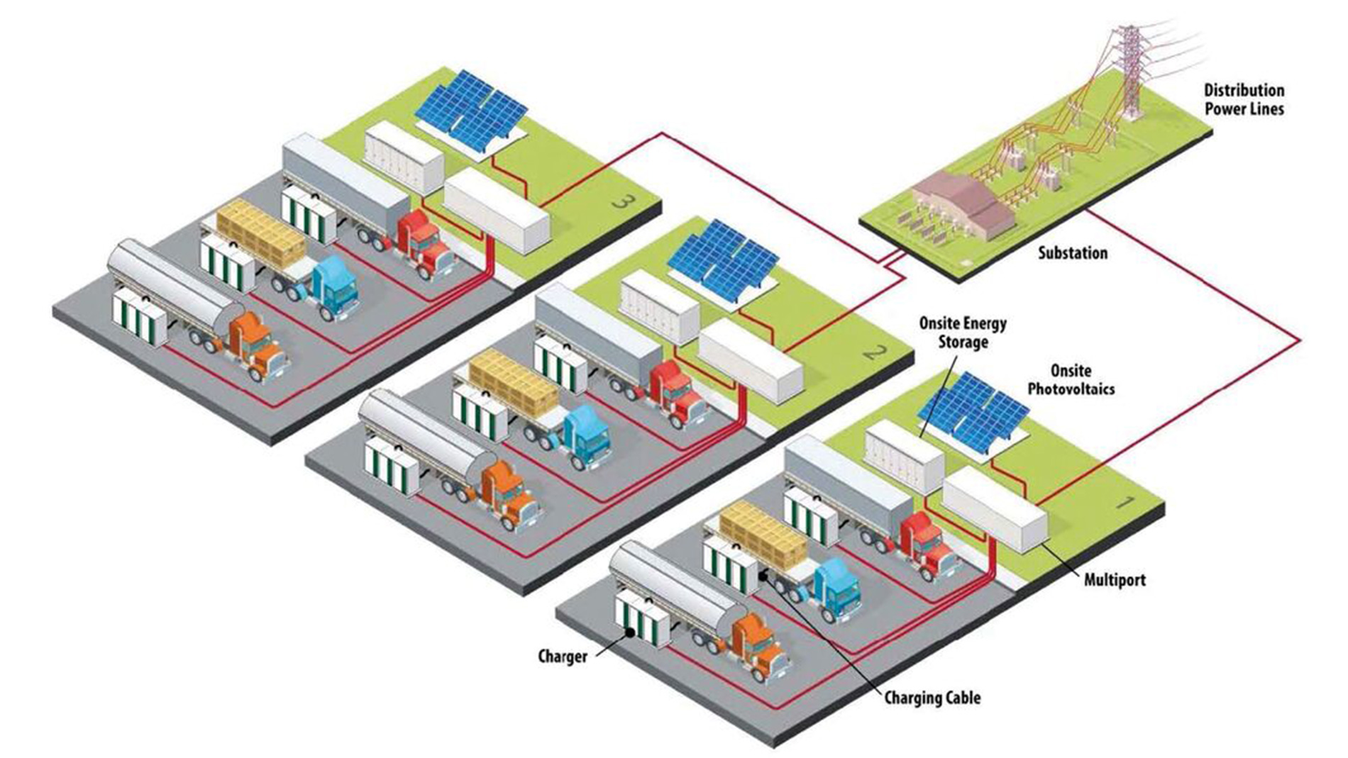
The Oak Ridge National Laboratory (ORNL) has proposed a multiport concept that illustrates such an architecture for megawatt charging. It connects multiple charging points, stationary energy storage systems, and photovoltaic installations via a shared electrical infrastructure. The entire charging station has a capacity of 10 to 15 MW; individual multiport units are designed to transmit power outputs of between 1 and 5 MW. A converter for heavy-duty electric vehicles has a rating of 1.2 MW and can supply either a single charging point with the full power or three charging points, each with 400 kW.
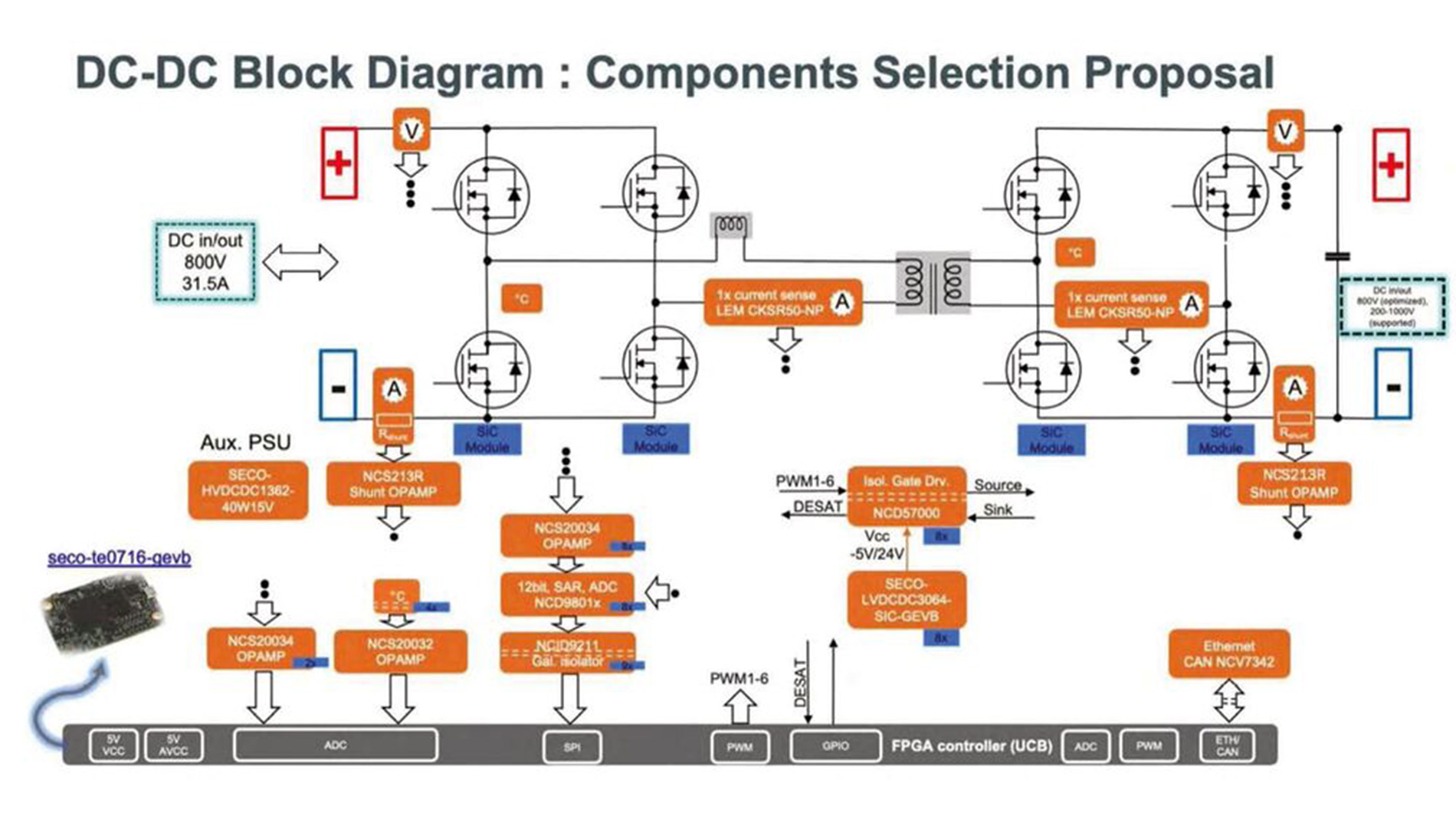
The concept provides a DC/DC stage in a dual-active-bridge topology for each charging point. A DAB consists of two actively controlled full bridges which are coupled to one another via a high-frequency transformer. The primary-side bridge generates a high-frequency AC voltage from the DC link voltage. Following galvanic isolation, the second bridge performs active rectification and provides a DC voltage on the vehicle side.
Since both sides have active power switches, energy can, in principle, be transferred in both directions. This means that a DAB can charge a vehicle battery and also transfer energy from a vehicle or stationary battery back into the shared DC system. Actively controlled semiconductors also enable synchronous rectification. During this process, the transistors perform the function of passive rectifier diodes, thereby reducing conduction losses.
Power transmission in a DAB is controlled via the phase shift in the time domain between the square-wave voltages of both bridges. The switching frequency can remain constant. This simplifies the design of the high-frequency transformer and the filters, as the main switching and interference components occur within defined frequency ranges. This control structure can also accommodate operation under varying loads.
Figure 1: ORNL Multiport Architecture (Image: Oak Ridge National Laboratory/onsemi)
From the three-phase mains supply to the DC intermediate circuit
On the mains side, an active three-phase power factor correction (PFC) stage handles the AC/DC conversion. This stage regulates the currents of the three mains phases, making them as sinusoidal and in phase with the respective voltages as possible. This improves the power factor while reducing the harmonic content of the input current. At the same time, the PFC stage stabilizes the DC bus voltage for the downstream DC/DC converters.
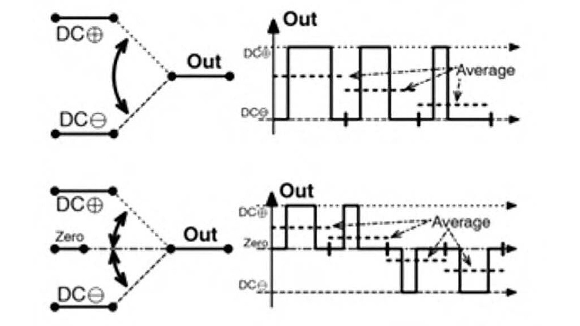
A T-type neutral-point-clamped topology is ideal for this active mains stage. This three-point circuit can connect a phase terminal to three different voltage potentials. Compared with a two-stage circuit, this results in smaller voltage steps. This reduces current ripple and facilitates filtering. Depending on their position within the circuit, individual semiconductors only need to switch a portion of the total intermediate circuit voltage.
Figure 2: DAB Block Diagram (Image: onsemi)
As charging power increases, integrated silicon carbide (SiC) power modules are becoming increasingly important. These modules combine several power switches of a given topology within a single package, enabling short electrical connections between the semiconductors. At the same time, their substrates establish a defined thermal link to the heat sink. This integration reduces parasitic inductances and aids the dissipation of heat generated by the semiconductors.
As charging power increases, cooling also becomes a key aspect of the system design. In addition to the power modules, active cooling of the cables and connectors may be necessary for very high charging currents. To facilitate this, a closed-loop liquid circuit pumps coolant through pipes running parallel to the power cables and on to the connector. The heat absorbed there is transported back to the charging station and transferred to the cooling system.
These requirements result in a two-stage, modular design. An active T-NPC stage connects the system to the three-phase mains supply and generates a regulated DC link voltage. Galvanically isolated DAB converters adapt this voltage for the vehicle battery and enable bidirectional energy flow. SiC power modules and liquid cooling help manage electrical and thermal loads.
Simulation of a separate 50 kW T-NPC input stage with a SiC power module yields an efficiency of 98.96 per cent at an input voltage of 400 V AC, an output voltage of 800 V DC, and a switching frequency of 20 kHz. At a heat sink temperature of 90 °C, the junction temperature reaches a maximum of 125.34 °C, with losses of 523.9 W reported for the module. It should be noted that these values are derived from a simulation and are different from the measurements on the 100 kW demonstrator described below.
Figure 3: Unlike a two-stage converter, a three-point topology can also produce a zero state. The smaller voltage steps reduce current ripple and make filtering easier. (Image: onsemi)
The Bidirectional 100 kW Demonstrator
onsemi’s 100 kW DC fast-charging demonstrator brings the above-described circuit concepts to life in a practical power unit. Designed as a bidirectional system, it supports the flow of energy from the grid to the vehicle and back again. Galvanic isolation between the grid and vehicle sides is an essential part of the safety concept for DC charging systems. A target peak efficiency of over 97 per cent has been specified.
The grid connection is three-phase with a protective earth conductor. The input voltage range extends from 400 to 600 V AC at frequencies between 40 and 70 Hz. The maximum phase current is specified as approximately 170 A_(eff). The overall specification states a voltage range of 680 to 1,500 V DC for the output.
For the input current, total harmonic distortion of no more than 5 per cent is specified at an output power of between 50 and 100 per cent. The specified power factor is at least 0.9 at 25–50% output power, at least 0.98 at 50–100% output power and at least 0.99 at rated power, rated input voltage and rated frequency.
The maximum switching frequency of the AC/DC stage is 70 kHz. The second harmonic should remain below 150 kHz when selecting the frequency; this is a specified design target in accordance with EN 55011 Class A and FCC Part 15 Class A. The DC/DC stage operates at 100 kHz.
Power electronics and thermal design
The system consists of a PFC stage and two DC/DC converters. The PFC stage uses three T-NPC SiC modules with 2 kV chips and a specified turn-on resistance of 8 mΩ. The two DAB units are each rated at 50 kW. Each unit contains four 1200 V SiC modules of the NXH003P120M3F2PTNG type with a specified on-resistance of 3 mΩ.
The power electronics are distributed across two circuit boards. The primary-side power board comprises the PFC stage and the primary sides of the two DAB converters. The secondary-side power circuit board houses the secondary sides of the DAB converters.
The power modules are liquid-cooled. A flow rate of 10 l/min and a maximum pressure drop of 120 mbar are specified for the heat sinks at a coolant temperature of 55 °C. The modules are connected to a standard cold plate via thermal interface material.
Assembly and commissioning
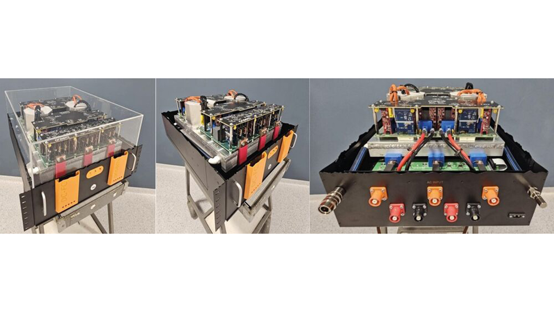
Testing of the 100 kW power unit begins with an initial prototype test of the individual circuit boards. This involves checking the component values and the quality of the solder joints, among other things. This is followed by commissioning tests to verify the functionality of the circuit boards.
When commissioning the PFC stage, the necessary components are installed first and the laboratory equipment is prepared. Testing then takes place in both rectifier and inverter modes. During this process, operational behaviour and efficiency are recorded. The DAB stages undergo a similar commissioning process.
The test plan comprises mechanical and visual inspections; commissioning of the individual circuit boards; testing of the mains input and AC/DC stage; commissioning of the DAB converters; and examination of the integrated system. It includes step-by-step load changes, variations in voltage and frequency, efficiency measurements and testing of fault and protection functions. These include overcurrent, overvoltage, undervoltage, and thermal overload. The system is controlled using an external real-time controller of the OPAL-RT OP4512 type.
PFC stage measurements
Power dissipation and efficiency were measured at the PFC stage. However, the intended output power of 100 kW could not be achieved for all combinations of input and output voltages. The junction temperature of the transistors was a limiting factor.
At an input voltage of 600 V AC, the minimum required output voltage increased to 860 V to keep the PFC stage in boost mode. Due to a limitation of the power analyzer used, the maximum output voltage was reduced from 1500 V to 1495 V for the measurements.
Measurements of the DAB stages
The power dissipation and efficiency of the two DAB stages were also determined. Initially, both converters were measured separately, with each achieving a maximum output power of 50 kW.
In order to cover a wide battery voltage range, the two DAB converters can be connected in parallel or in series on the vehicle side. They operate in parallel at battery voltages of 425 to 750 V. A series connection is provided for voltages between 850 and 1,500 V, and a transition range between 750 and 850 V exists where both connection configurations are possible in principle. However, the DAB stages operate outside their ideal voltage ratio of 1:1 within this range. In this cases the more favorable configuration should be determined based on efficiency rating.
Thus the description of the operating modes extends down to 425 V on the battery side, hence the overarching specification states an output voltage range of 680 to 1,500 V DC. The documentation does not explain these differing figures in detail.
There are four operating modes:
- Charging the battery with DAB stages connected in series;
- Charging the battery with DAB stages connected in parallel;
- Inverter operation with DAB stages connected in series;
- Inverter operation with DAB stages connected in parallel.
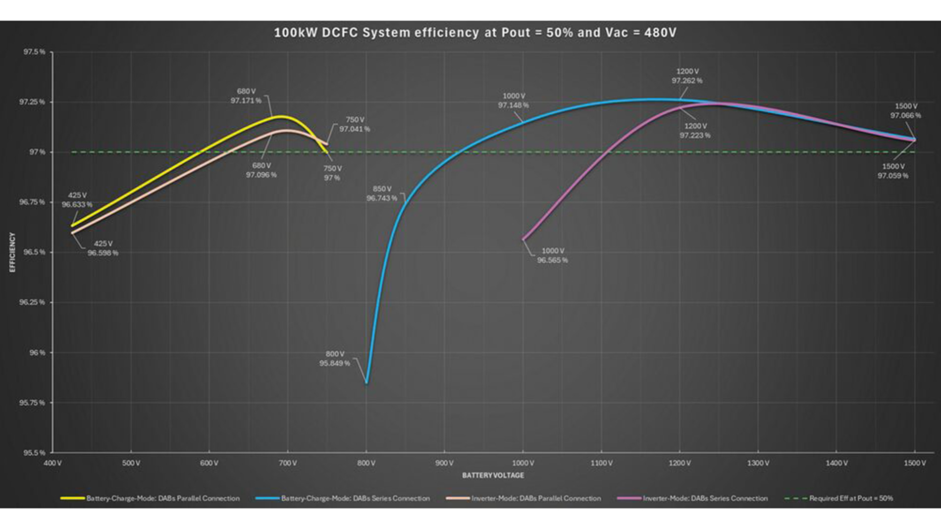
In inverter mode, the operating points could not be measured at battery voltages of 800 V and 850 V. Above 750 V, the centre point of the DC intermediate circuit became unbalanced. Summary efficiency measurements of the complete system were carried out at a transmitted power of 50 kW and a three-phase mains voltage of 480 V, and at most of the investigated operating points, the measured efficiency was above the specified minimum value. Reducing the gate resistances of the SiC modules in the PFC and DAB stages is suggested as a way of improving efficiency further. This adjustment is planned to optimize the system further.
Figure 5: 100 kW DC Fast Charger Total System Efficiency at 50% Power ans Vac 480 V (Image: onsemi)
Further development required
The 100 kW power unit incorporates SiC power modules alongside measurement, control and protection functions within a bidirectional configuration. Connecting the two DAB converters in series or parallel enables operation across a wide battery voltage range.
Further development is required in terms of the thermal behavior of the SiC modules in the PFC stage and the transformers in the DAB converters. The stability of the control algorithms also needs to be improved further. Mechanical optimization could reduce the size and weight of the assembly by 25–30%. Further work is planned to determine how the system can be revised to fully achieve the intended performance targets. St