In Search of the “Killer App” for Bidirectional GaN: Something Entirely New in Power Electronics
27 Oct 2026
The introduction of bidirectional power semiconductors based on GaN and SiC could be described as a step into a brand-new era. Instead of having to rely on multilevel topologies, bidirectional designs can now be implemented much more easily. That said, the number of current applications remains quite limited.
Improving what already exists this has been the guiding principle for the mainstream of electronics development, including in the semiconductor sector. Higher efficiency, lower losses, and increased power density have essentially been the “holy trinity” of power electronics over the last few decades. While new semiconductor technologies like SiC and GaN have provided an additional boost to these efforts, the underlying system architectures of power electronics have remained largely unchanged.
For this reason, it drew significant attention when, at PCIM 2025, three prominent power semiconductor manufacturers introduced something entirely new in the 650 V range: bidirectional GaN switches. Unlike conventional approaches, these new offerings did not merely represent an incremental improvement over existing silicon-based solutions. Instead, they provided engineers with the opportunity to fundamentally rethink how electrical energy is routed, controlled, stored, and converted within an entire power supply system.
Their ability to control current flow in both directions switching positive and negative half-cycles directly eliminates the need for additional anti-parallel diodes or extra FETs. This makes bidirectional power semiconductors, such as the 650 V GaN switches unveiled by Infineon Technologies, Renesas, and Navitas, ideal for applications like AC/DC converters, solid-state switches, and bidirectional power supplies, without requiring the use of multi-level topologies. Furthermore, employing these bidirectional switches not only reduces the required chip area on the board but also lowers conduction losses, as there is only a single, shared depletion region.
Creating a bidirectional flow of current was already possible, but it previously required significantly more components than are needed with today’s highly integrated GaN solutions. “The true value of this technology extends far beyond performance at the component level,” argues Mirco Drews, Senior Manager of Strategic Business Development at Nexperia. “The greatest impact of these components will be felt at the system level, where they will enable entirely new power architectures in the future.”
"The true value of bidirectional power semiconductors extends far beyond conventional solutions; these new components will have their greatest impact at the system level, where they will enable the realization of entirely new power architectures in the future."
While energy was traditionally routed from source to load along a fixed path, this process will become significantly more dynamic in the future. It is expected that future systems will essentially exist in a constant state of balancing a continuous redistribution between energy storage and energy reuse, depending on specific operating conditions. Bidirectional GaN switches are set to play a key role in these future applications.
On the board, the use of bidirectional GaN power semiconductors not only saves chip area but also reduces conduction losses, as there is only a single shared depletion zone. Consequently, their implementation lowers both the potential design costs for an application and the number of components required for its realization which, in turn, impacts inventory requirements. For this reason, it was already clear by 2025 that 650V bidirectional GaN power semiconductors would help achieve significant cost savings at the system level.
While bidirectional GaN power semiconductors did exist previously, they were limited to low-voltage versions. According to Dr. Gerald Deboy, a Fellow at Infineon Technologies Austria, the key difference in the now-available high-voltage versions lies in substrate stabilization: “This helps improve isolation between the components and increases the breakdown voltage. Highly insulating materials, such as SiC or sapphire, can be used for this purpose.”
"In the high-voltage version of bidirectional GaN power semiconductors, substrate stabilization is of critical importance. It helps to improve isolation between components and increase the breakdown voltage. Highly insulating materials, such as SiC or sapphire, are well-suited for this purpose."
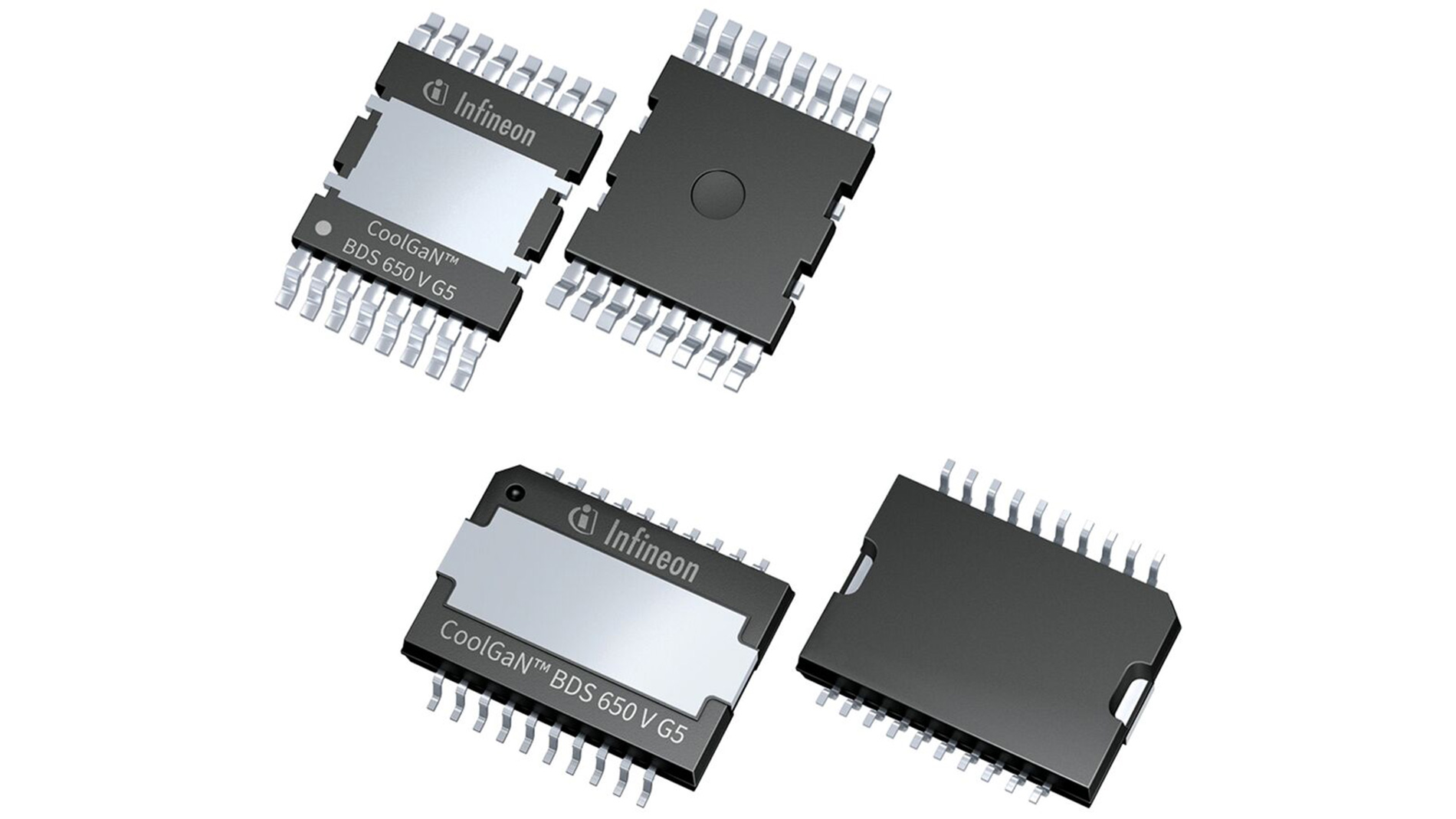
More than a year ago, Infineon Technologies introduced its 650 V bidirectional GaN power semiconductors, featuring a common-drain design and a dual-gate structure. These components leverage the company’s robust gate-injection transistor technology to provide a monolithic bidirectional switch capable of actively blocking both voltage and current in either direction. There is no doubt that such switches could enable innovative battery architectures for instance, in electric vehicles. They would, for example, allow for the dynamic control of individual battery modules based on their “state of health” and specific operating conditions. This advancement would make it possible to improve battery utilization while simultaneously enhancing the robustness of the overall system.
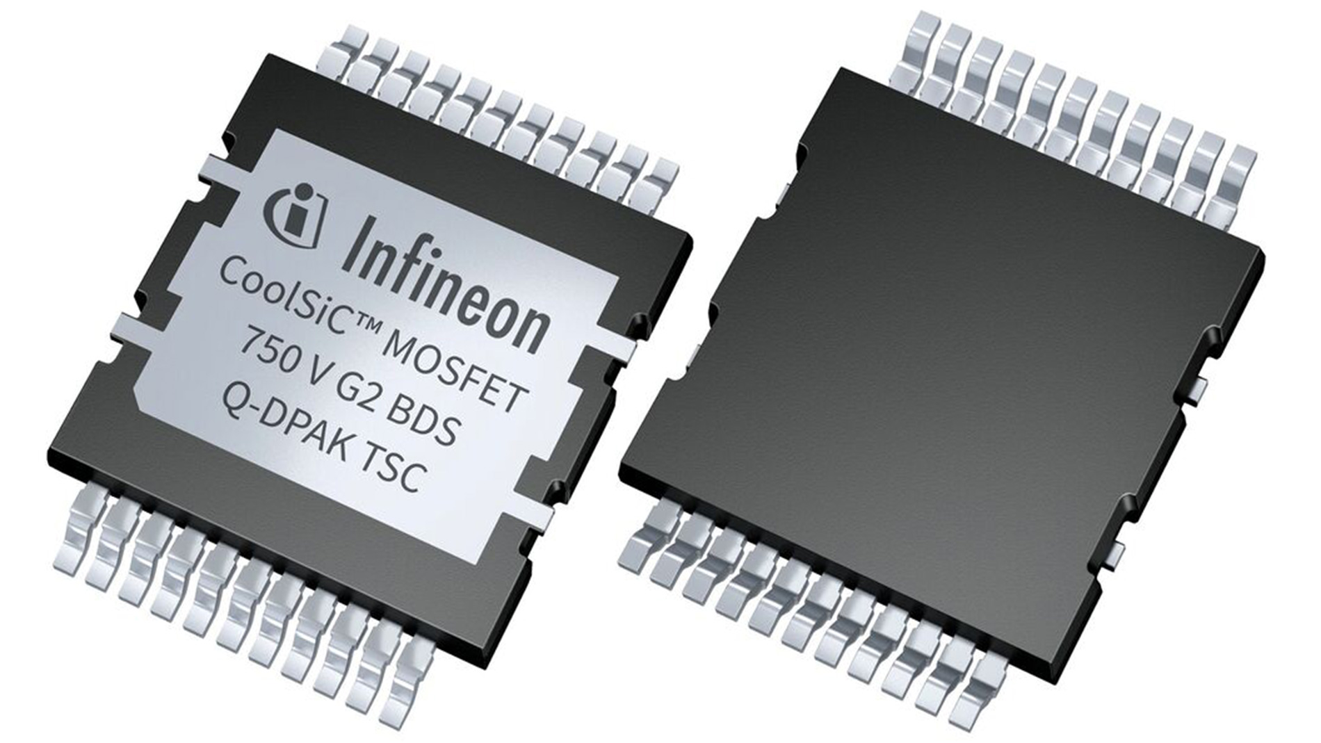
Since PCIM 2026, Infineon Technologies has been pursuing a dual-track strategy regarding bidirectional power semiconductors. In addition to the 650 V CoolGaN Bidirectional Switch (BDS) (left)—which was introduced the previous year the company unveiled the SiC variants of its 750 V CoolSiC BDS series (right) at this year’s PCIM (Images: Infineon Technologies).
According to Nexperia executive Drews, the true value of bidirectional GaN power semiconductors lies in shifting the focus of innovation moving away from optimizing individual power stages toward redesigning the entire system architecture. “Instead of simply continuing to shrink existing converters and make them more efficient, engineers can use these new bidirectional components to explore entirely fresh approaches to energy management, protection schemes, power distribution, and power conversion.”
Are these possibilities actually being embraced by developers? If you ask one of the three innovators, Navitas Semiconductor, they point out that their bidirectional 650 V GaN power semiconductors are currently being used in solar microinverters from Enphase Energy though they were already being used there last year. When the market potential for these products is discussed, the aforementioned applications are frequently cited, yet no one explicitly confirms that they are actively pursuing this approach. As of today, no other suppliers of such solutions have entered the market, even though several prominent power semiconductor manufacturers had previously indicated that they were working on similar products. Perhaps not enough time has passed for developers to truly explore the new possibilities offered by bidirectional GaN power semiconductors?
Of course, bidirectional power semiconductors can be implemented using materials other than GaN for instance, SiC. Infineon Technologies has taken this route, unveiling the industry’s first SiC bidirectional switches at this year’s PCIM exhibition. These are based on the company’s 750 V CoolSiC G2 technology, which combines a vertically integrated dual-die design featuring a common-drain configuration into a single component housed in a top-side cooled Q-DPAK package.
According to the manufacturer, these components offer excellent RDS(on) x Qfr and RDS(on) x QOSS figures, as well as a low Qg. Consequently, switching and conduction losses are reduced, enabling ultra-fast and efficient switching.
Infineon states that a typical VGS(th) of 4.5 V at +25 °C, combined with a very low QGD-to-QGS ratio, increases immunity against parasitic turn-on. Meanwhile, an extended gate-bias tolerance ranging from -11 V to 25 V enhances design flexibility and the compatibility of these power semiconductors. With a voltage rating of 200 V/ns, these devices support high-frequency designs without requiring any compromises in terms of longevity.
As for potential applications, these bidirectional components are particularly well-suited for automotive use specifically in on-board chargers, EV charging systems, eFuse circuits, and pre-charge circuits. For instance, when paired with a CoolSiC H-DPAK half-bridge, they facilitate a seamless transition to single-stage, SiC-based on-board chargers, enabling designs that offer exceptionally high power density while remaining space- and cost-efficient. eg